LTC3531-3.3

Features: ` Regulated Output with Input Above, Below or Equal to the Output` Single Inductor` Up to 90% Effi ciency` VIN Range: 1.8V to 5.5V` 200mA at 3.3VOUT from 3.6V Input` 125mA at 3VOUT from 2.5V Input` Fixed VOUT Versions (TSOT, DFN): 3.3V, 3V` Adjustable VOUT Version (DFN): 2V to 5V` Burst ...

product image

LTC3531-3.3 Picture
SeekIC No. : 004402271 Detail

LTC3531-3.3: Features: ` Regulated Output with Input Above, Below or Equal to the Output` Single Inductor` Up to 90% Effi ciency` VIN Range: 1.8V to 5.5V` 200mA at 3.3VOUT from 3.6V Input` 125mA at 3VOUT from 2....

floor Price/Ceiling Price

Part Number:
LTC3531-3.3
Supply Ability:
5000

Price Break

  • Qty
  • 1~5000
  • Unit Price
  • Negotiable
  • Processing time
  • 15 Days
Total Cost: $ 0.00

SeekIC Buyer Protection PLUS - newly updated for 2013!

  • Escrow Protection.
  • Guaranteed refunds.
  • Secure payments.
  • Learn more >>

Month Sales

268 Transactions

Rating

evaluate  (4.8 stars)

Upload time: 2024/5/27

Payment Methods

All payment methods are secure and covered by SeekIC Buyer Protection PLUS.

Notice: When you place an order, your payment is made to SeekIC and not to your seller. SeekIC only pays the seller after confirming you have received your order. We will also never share your payment details with your seller.
Product Details

Description


Features:

` Regulated Output with Input Above, Below or Equal to the Output
` Single Inductor
` Up to 90% Effi ciency
` VIN Range: 1.8V to 5.5V
` 200mA at 3.3VOUT from 3.6V Input
` 125mA at 3VOUT from 2.5V Input
` Fixed VOUT Versions (TSOT, DFN): 3.3V, 3V
` Adjustable VOUT Version (DFN): 2V to 5V
` Burst Mode® Operation, No External Compensation
` Ultra Low Quiescent Current: 16A, Shutdown Current <1A
` Only 3 External Components Required
` Short-Circuit Protection
` Output Disconnect in Shutdown
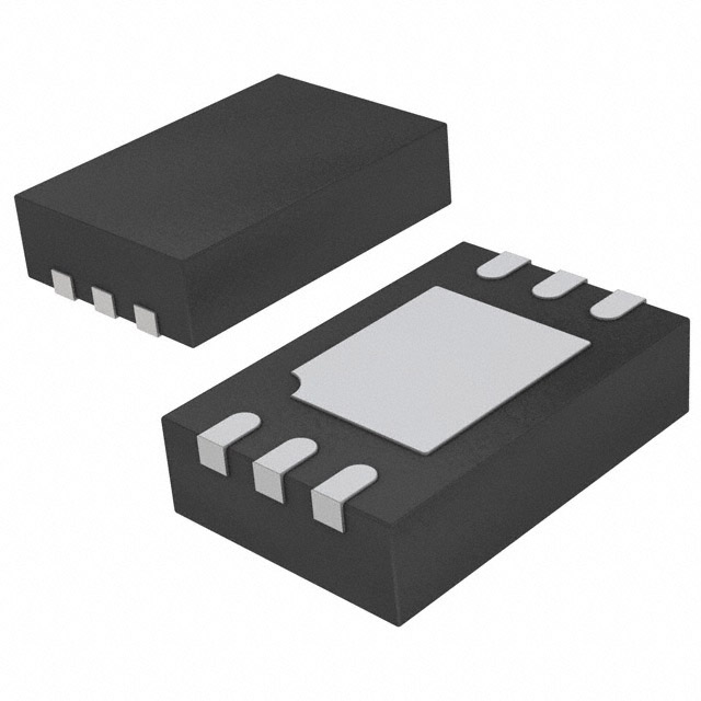
` Available in 6-Pin ThinSOT and 3mm * 3mm DFN Packages


Application

· Handheld Instruments
·MP3 Players
· Handheld computers
· PDA/GPS


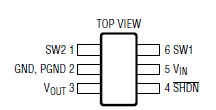
Pinout

  Connection Diagram


Specifications

VIN, VOUT, SWA, SWB, SHDN Voltage ................0.3 to 6V
SWA, SWB Voltage, <100ns Pulse .....................0.3 to 7V
Operating Temperature Range (Note 2) ... 40°C to 85°C
Storage Temperature Range .................. 65°C to 125°C
Lead Temperature (TS6, Soldering, 10 sec) ............. 300°C


Description

The LTC®3531/LTC3531-3.3/LTC3531-3 are synchronous buck-boost DC/DC converters that operate from input voltages above, below or equal to the output voltage. The topology incorporated in the ICs provides a continuous transfer through all operating modes, making the product ideal for single cell Li-Ion and multicell alkaline or nickel applications. The converters operate in Burst Mode, minimizing solution footprint and component count as well as providing high conversion effi ciency over a wide range of load currents.

The LTC3531/LTC3531-3.3/LTC3531-3 include two 0.5 N-channel MOSFET switches and two P-channel switches (0.5, 0.8). Quiescent current is typically 16A, making the parts ideal for battery power applications. Other features include a <1A shutdown current, current limiting, thermal shutdown and output disconnect. The parts are offered in a 6-pin ThinSOTTM package for fi xed voltage versions or a 3mm * 3mm DFN package for fi xed and adjustable versions.


Customers Who Bought This Item Also Bought

Margin,quality,low-cost products with low minimum orders. Secure your online payments with SeekIC Buyer Protection.