LTC3408

Features: Dynamically Adjustable Output from 0.3V to 3.5V 600mA Output Current Internal 0.08Ω P-Channel MOSFET Bypass Transistor High Efficiency: Up to 96% 1.5MHz Constant Frequency Operation No Schottky Diode Required Low Dropout Operation: 100% Duty Cycle 2.5V to 5V Input Voltage Range Sh...

product image

LTC3408 Picture
SeekIC No. : 004402219 Detail

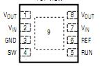
LTC3408: Features: Dynamically Adjustable Output from 0.3V to 3.5V 600mA Output Current Internal 0.08Ω P-Channel MOSFET Bypass Transistor High Efficiency: Up to 96% 1.5MHz Constant Frequency Operation...

floor Price/Ceiling Price

Part Number:
LTC3408
Supply Ability:
5000

Price Break

  • Qty
  • 1~5000
  • Unit Price
  • Negotiable
  • Processing time
  • 15 Days
Total Cost: $ 0.00

SeekIC Buyer Protection PLUS - newly updated for 2013!

  • Escrow Protection.
  • Guaranteed refunds.
  • Secure payments.
  • Learn more >>

Month Sales

268 Transactions

Rating

evaluate  (4.8 stars)

Upload time: 2024/5/22

Payment Methods

All payment methods are secure and covered by SeekIC Buyer Protection PLUS.

Notice: When you place an order, your payment is made to SeekIC and not to your seller. SeekIC only pays the seller after confirming you have received your order. We will also never share your payment details with your seller.
Product Details

Description


Features:

Dynamically Adjustable Output from 0.3V to 3.5V
600mA Output Current
Internal 0.08Ω P-Channel MOSFET Bypass Transistor
High Efficiency: Up to 96%
1.5MHz Constant Frequency Operation
No Schottky Diode Required
Low Dropout Operation: 100% Duty Cycle
2.5V to 5V Input Voltage Range
Shutdown Mode Draws < 1µA Supply Current
Current Mode Operation for Excellent Line and
Load Transient Response
Overtemperature Protected
Available in 8-Lead 3mm * 3mm DFN Package


Application

WCDMA Cell Phone Power Amplifiers
Wireless Modems


Pinout

  Connection Diagram


Specifications

Input Supply Voltage (<300µs) ..................  0.3V to 6V
Input Supply Voltage (DC) .......................  0.3V to 5.5V
RUN, REF, VOUT Voltages ..........................  0.3V to VIN
SW Voltage (DC) .........................  0.3V to (VIN + 0.3V)
P-Channel Switch Source Current (DC) ..............  800mA
N-Channel Switch Sink Current (DC) ..................  800mA
Peak SW Sink and Source Current .........................  1.3A
Bypass P-Channel FET Source Current (DC) .............. 1A
Operating Temperature Range (Note 2) .40°C to 85°C
Junction Temperature (Note 3) ............................  125°C
Storage Temperature Range ............... 65°C to 125°C


Description

The LTC®3408 is a high efficiency monolithic synchro- nous buck regulator optimized for WCDMA power ampli- fier applications. The output voltage can be dynamically programmed from 0.3V to 3.5V. At VOUT > 3.6V an internal 0.08Ω bypass P-channel MOSFET connects VOUT directly to VIN, eliminating power loss through the inductor.

The input voltage range is 2.5V to 5V making the LTC3408 ideally suited for single Li-Ion battery-powered applica-tions. 100% duty cycle provides low dropout operation,extending battery life in portable systems.

Switching frequency is internally set at 1.5MHz, allowing the use of small surface mount inductors and capacitors.

The internal synchronous switch increases efficiency and eliminates the need for an external Schottky diode.

The LTC3408 is available in a low profile (0.75mm) 8-lead 3mm × 3mm DFN package.


Customers Who Bought This Item Also Bought

Margin,quality,low-cost products with low minimum orders. Secure your online payments with SeekIC Buyer Protection.
Hardware, Fasteners, Accessories
Transformers
Circuit Protection
Tapes, Adhesives
803
View more