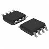
Features: ` Tiny 3mm * 3mm 8-Pin DFN Package` Maximum 16-Bit INL Error: ±2LSB over Temperature` Low 120A Supply Current` Guaranteed Monotonic over Temperature` Low 0.5nV•sec Glitch Impulse` 2.7V to 5.5V Single Supply Operation` Fast 1s Settling Time to 16 Bits` Unbuffered Voltage Output Dire...
LTC2641: Features: ` Tiny 3mm * 3mm 8-Pin DFN Package` Maximum 16-Bit INL Error: ±2LSB over Temperature` Low 120A Supply Current` Guaranteed Monotonic over Temperature` Low 0.5nV•sec Glitch Impulse` 2....
SeekIC Buyer Protection PLUS - newly updated for 2013!
268 Transactions
All payment methods are secure and covered by SeekIC Buyer Protection PLUS.
VDD to GND .................................................0.3V to 6V
CS, SCLK, DIN,
CLR to GND ........................0.3V to (VDD + 0.3V) or 6V
REF, VOUT, INV to GND ......0.3V to (VDD + 0.3V) or 6V
RFB to INV .................................................... 6V to 6V
RFB to GND ....................................................6V to 6V
Operating Temperature Range
LTC2641C/LTC2642C ................................... 0 to 70
LTC2641I/LTC2642I ................................ 40 to 85
Maximum Junction Temperature ........................... 125
Storage Temperature Range ..................65 to 150
Lead Temperature (Soldering, 10 sec) .................. 300
The LTC®2641/LTC2642 are families of 16-, 14- and 12-bit unbuffered voltage output DACs. These DACs operate from a single 2.7V to 5.5V supply and are guaranteed monotonic over temperature. The LTC2641-16/LTC2642-16 provide 16-bit performance (±2LSB INL and ±1LSB DNL) over temperature. Unbuffered DAC outputs result in low supply current of 120A and a low offset error of ±1LSB.
Both the LTC2641 and LTC2642 feature a reference input range of 2V to VDD. VOUT swings from 0V to VREF. For bipolar operation, the LTC2642 includes matched scaling resistors for use with an external precision op amp (such as the LT1678), generating a ±VREF output swing at RFB.
The LTC2641/LTC2642 use a simple SPI/MICROWIRE compatible 3-wire serial interface which can be operated at clock rates up to 50MHz and can interface directly with optocouplers for applications requiring isolation. A power-on reset circuit clears the LTC2641's DAC output to zero scale and the LTC2642's DAC output to midscale when power is initially applied. A logic low on the CLR pin asynchronously clears the DAC to zero scale (LTC2641) or midscale (LTC2642). These DACs are all specifi ed over the commercial and industrial ranges.