SeekIC No. : 004402107
Detail
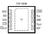
LTC2611: Features: Smallest Pin-Compatible Single DACs: LTC2601: 16 Bits LTC2611: 14 Bits LTC2621: 12 BitsGuaranteed Monotonic Over Temperature Wide 2.5V to 5.5V Supply RangeLow Power Operation: 300µA...
 LTC2611 Data Sheet
floor Price/Ceiling Price
- Part Number:
- LTC2611
- Supply Ability:
- 5000
Price Break
- Qty
- 1~5000
- Unit Price
- Negotiable
- Processing time
- 15 Days
SeekIC Buyer Protection PLUS - newly updated for 2013!
- Escrow Protection.
- Guaranteed refunds.
- Secure payments.
- Learn more >>
Month Sales
268 Transactions
Payment Methods
All payment methods are secure and covered by SeekIC Buyer Protection PLUS.
Notice: When you place an order, your payment is made to SeekIC and not to your seller. SeekIC only pays the seller after confirming you have received your order. We will also never share your payment details with your seller.