LTC17515

Features: 5V Output Current: 100mA (VIN ³ 3V)3.3V Output Current: 80mA (VIN ³ 2.5V)Ultralow Power: 20mA Quiescent CurrentRegulated Output Voltage: 3.3V ±4%, 5V ±4%, ADJVIN Range: 2V to 5.5V800kHz Switching FrequencyNo InductorsVery Low Shutdown Current: <2mAShutdown Disconnects Load f...

product image

LTC17515 Picture
SeekIC No. : 004401882 Detail

LTC17515: Features: 5V Output Current: 100mA (VIN ³ 3V)3.3V Output Current: 80mA (VIN ³ 2.5V)Ultralow Power: 20mA Quiescent CurrentRegulated Output Voltage: 3.3V ±4%, 5V ±4%, ADJVIN Range: 2V to 5.5...

floor Price/Ceiling Price

Part Number:
LTC17515
Supply Ability:
5000

Price Break

  • Qty
  • 1~5000
  • Unit Price
  • Negotiable
  • Processing time
  • 15 Days
Total Cost: $ 0.00

SeekIC Buyer Protection PLUS - newly updated for 2013!

  • Escrow Protection.
  • Guaranteed refunds.
  • Secure payments.
  • Learn more >>

Month Sales

268 Transactions

Rating

evaluate  (4.8 stars)

Upload time: 2025/1/10

Payment Methods

All payment methods are secure and covered by SeekIC Buyer Protection PLUS.

Notice: When you place an order, your payment is made to SeekIC and not to your seller. SeekIC only pays the seller after confirming you have received your order. We will also never share your payment details with your seller.
Product Details

Description


Features:

 5V Output Current: 100mA (VIN ³ 3V)
 3.3V Output Current: 80mA (VIN ³ 2.5V)
 Ultralow Power: 20mA Quiescent Current
 Regulated Output Voltage: 3.3V ±4%, 5V ±4%, ADJ
 VIN Range: 2V to 5.5V
 800kHz Switching Frequency
 No Inductors
 Very Low Shutdown Current: <2mA
 Shutdown Disconnects Load from VIN
 PowerGood/Undervoltage Output
 Adjustable Soft-Start Time
 Short-Circuit/Thermal Protection
 Available in 8-Pin MSOP


Application

 SIM Interface Supplies for GSM Cellular Telephones
 Li-Ion Battery Backup Supplies
 Local 3V and 5V Conversion
 Smart Card Readers
 PCMCIA Local 5V Supplies
 White LED Backlighting


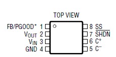
Pinout

  Connection Diagram


Specifications

VIN to GND ............................................................................. 0.3V to 6V
PGOOD, FB, VOUT to GND ....................................................... 0.3V to 6V
SS, SHDN to GND ..................................................... 0.3V to (VIN + 0.3V)
VOUT Short-Circuit Duration ....................................................... Indefinite
IOUT (Note 2).................................................................................. 125mA
Operating Temperature Range (Note 3) ............................. 40°C to 85°C
Storage Temperature Range ............................................ 65°C to 150°C
Lead Temperature (Soldering, 10 sec).............................................. 300°C


Description

The LTC®1751 family of products are micropower charge pump DC/DC converters that produce a regulated output voltage. The input voltage range is 2V to 5.5V. Extremely low operating current (20mA typical with no load) and low external parts count (one flying capacitor and two small bypass capacitors at VIN and VOUT) make them ideally suited for small, battery-powered applications.

The LTC1751 family operate as Burst ModeTM switched capacitor voltage doublers to achieve ultralow quiescent current. They have thermal shutdown capability and can survive a continuous short circuit from VOUT to GND. The PGOOD pin on the LTC1751-3.3 and LTC1751-5 indicates when the output voltage has reached its final value and if the output has an undervoltage fault condition. The FB pin of the adjustable LTC1751 can be used to program the desired output voltage or current. An optional soft-start capacitor may be used at the SS pin to prevent excessive inrush current during start-up.

The LTC1751 family is available in an 8-pin MSOP package.


Customers Who Bought This Item Also Bought

Margin,quality,low-cost products with low minimum orders. Secure your online payments with SeekIC Buyer Protection.
Cables, Wires - Management
Undefined Category
Transformers
Isolators
Memory Cards, Modules
Fans, Thermal Management
View more