LTC1750

Features: `Sample Rate: 80Msps`500MHz Full Power Bandwidth S/H`Direct IF Sampling Up to 500MHz`PGA Front End (2.25VP-P or 1.35VP-P Input Range)`75.5dB SNR and 90dB SFDR (PGA = 0)`73dB SNR and 90dB SFDR (PGA = 1)`No Missing Codes`Single 5V Supply`Power Dissipation: 1.45W`Two Pin Selectable Referenc...

product image

LTC1750 Picture
SeekIC No. : 004401878 Detail

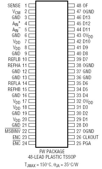
LTC1750: Features: `Sample Rate: 80Msps`500MHz Full Power Bandwidth S/H`Direct IF Sampling Up to 500MHz`PGA Front End (2.25VP-P or 1.35VP-P Input Range)`75.5dB SNR and 90dB SFDR (PGA = 0)`73dB SNR and 90dB S...

floor Price/Ceiling Price

Part Number:
LTC1750
Supply Ability:
5000

Price Break

  • Qty
  • 1~5000
  • Unit Price
  • Negotiable
  • Processing time
  • 15 Days
Total Cost: $ 0.00

SeekIC Buyer Protection PLUS - newly updated for 2013!

  • Escrow Protection.
  • Guaranteed refunds.
  • Secure payments.
  • Learn more >>

Month Sales

268 Transactions

Rating

evaluate  (4.8 stars)

Upload time: 2024/7/15

Payment Methods

All payment methods are secure and covered by SeekIC Buyer Protection PLUS.

Notice: When you place an order, your payment is made to SeekIC and not to your seller. SeekIC only pays the seller after confirming you have received your order. We will also never share your payment details with your seller.
Product Details

Description


Features:

`Sample Rate: 80Msps
`500MHz Full Power Bandwidth S/H
`Direct IF Sampling Up to 500MHz
`PGA Front End (2.25VP-P or 1.35VP-P Input Range)
`75.5dB SNR and 90dB SFDR (PGA = 0)
`73dB SNR and 90dB SFDR (PGA = 1)
`No Missing Codes
`Single 5V Supply
`Power Dissipation: 1.45W
`Two Pin Selectable Reference Values
`Two's Complement or Offset Binary Outputs
`Out-of-Range Indicator
`Data Ready Output Clock
`48-Pin TSSOP Package


Application

·Telecommunications
·Receivers
·Cellular Base Stations
·Spectrum Analysis
·Imaging Systems
·MRI
·Tomography


Pinout

  Connection Diagram


Specifications

OVDD = VDD (Notes 1, 2)
Supply Voltage (VDD) ............................................. 5.5V
Analog Input Voltage (Note 3) ... 0.3V to (VDD + 0.3V)
Digital Input Voltage (Note 4) .... 0.3V to (VDD + 0.3V)
Digital Output Voltage .............. 0.3V to (VDD + 0.3V)
OGND Voltage.............................................0.3V to 1V
Power Dissipation .......................................... 2000mW
Operating Temperature Range
LTC1750C ............................................... 0°C to 70°C
LTC1750I............................................ 40°C to 85°C
Storage Temperature Range ........... 65°C to 150°C
Lead Temperature (Soldering, 10 sec)................300°C


Description

The LTC®1750 is an 80Msps, 14-bit A/D converter designed for digitizing wide dynamic range signals up to frequencies of 500MHz. The input range of the ADC can be optimized with the on-chip PGA sample-and-hold circuit and flexible reference circuitry.

The LTC1750 has a highly linear sample-and-hold circuit with a bandwidth of 500MHz. The SFDR is 82dB with an input frequency of 250MHz. Ultralow jitter of 0.12psRMS allows undersampling of IF frequencies with minimal degradation in SNR. DC specs include ±3LSB INL and no missing codes.

The digital interface of LTC1750 is compatible with 5V, 3V, 2V and LVDS logic systems. The ENC and ENC inputs may be driven differentially from PECL, GTL and other low swing logic families or from single-ended TTL or CMOS. The low noise, high gain ENC and ENC inputs may also be driven by a sinusoidal signal without degrading performance. A separate output power supply can be operated from 0.5V to 5V, making it easy to connect directly to any low voltage DSPs or FIFOs.

The 48-pin TSSOP package with a flow-through pinout simplifies the board layout.


Customers Who Bought This Item Also Bought

Margin,quality,low-cost products with low minimum orders. Secure your online payments with SeekIC Buyer Protection.
Test Equipment
Circuit Protection
Fans, Thermal Management
Programmers, Development Systems
LED Products
View more