Features: ·Sample Rate: 80Msps
·76.3dB SNR and 90dB SFDR (3.2V Range)
·72.6dB SNR and 90dB SFDR (2V Range)
·No Missing Codes
·Single 5V Supply
·Power Dissipation: 1.4W
·Selectable Input Ranges: ±1V or ±1.6V
·240MHz Full Power Bandwidth S/H
·Pin Compatible Family
·25Msps: LTC1746 (14-Bit), LTC1745 (12-Bit)
·50Msps: LTC1744 (14-Bit), LTC1743 (12-Bit)
·65Msps: LTC1742 (14-Bit), LTC1741 (12-Bit)
·80Msps: LTC1748 (14-Bit), LTC1747 (12-Bit)
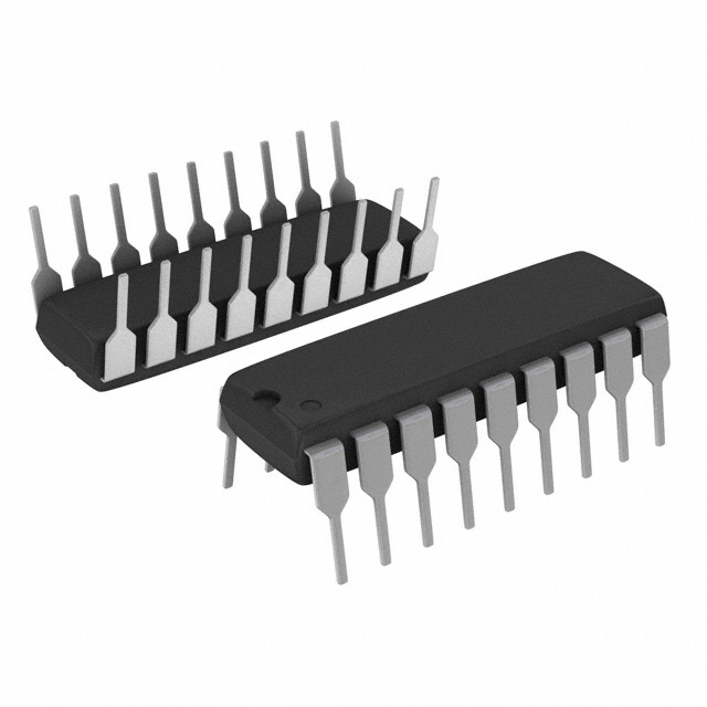
·48-Pin TSSOP PackageApplication·Telecommunications
·Receivers
·Cellular Base Stations
·Spectrum Analysis
·Imaging SystemsPinout SpecificationsOVDD = VDD (Notes 1, 2)
Supply Voltage (VDD) .............................................. 5.5V
Analog Input Voltage (Note 3) .... 0.3V to (VDD + 0.3V)
Digital Input Voltage (Note 4) ..... 0.3V to (VDD + 0.3V)
Digital Output Voltage ................. 0.3V to (VDD + 0.3V)
OGND Voltage............................................... 0.3V to 1V
Power Dissipation ............................................ . 2000mW
Operating Temperature Range
LTC1748C ............................................... . .0°C to 70°C
LTC1748I............................................ . 40°C to 85°C
Storage Temperature Range ...............65°C to 150°C
Lead Temperature (Soldering, 10 sec).................. 300°CDescriptionThe LTC
®1748 is an 80Msps, sampling 14-bit A/D converter designed for digitizing high frequency, wide dynamic range signals. Pin selectable input ranges of ±1V and ±1.6V along with a resistor programmable mode allow the LTC1748's input range to be optimized for a wide variety of applications.
The LTC1748 is perfect for demanding communications applications with AC performance that includes 76.3dB SNR and 90dB spurious free dynamic range. Ultralow jitter of 0.15psRMS allows undersampling of IF frequencies with excellent noise performance. DC specs include ±3LSB INL and no missing codes.
The digital interface of LTC1748 is compatible with 5V, 3V, 2V and LVDS logic systems. The ENC and ENC inputs may be driven differentially from PECL, GTL and other low swing logic families or from single-ended TTL or CMOS. The low noise, high gain ENC and ENC inputs may also be driven by a sinusoidal signal without degrading performance. A separate output power supply can be operated from 0.5V to 5V, making it easy to connect directly to any low voltage DSPs or FIFOs.
The TSSOP package with a flow-through pinout simplifies the board layout.

 LTC1748 Data Sheet


