LTC1555L

Features: Buck/Boost Charge Pump Generates 3V or 5VInput Voltage Range: 2.6V to 6VController VCC Range: 1.425V to 4.4V>10kV ESD on All SIM Contact PinsShort-Circuit and Overtemperature Protected3V to 5V Signal Level TranslatorsVery Low Operating Current: 40mAVery Low Shutdown Current: <1mASo...

product image

LTC1555L Picture
SeekIC No. : 004401686 Detail

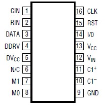
LTC1555L: Features: Buck/Boost Charge Pump Generates 3V or 5VInput Voltage Range: 2.6V to 6VController VCC Range: 1.425V to 4.4V>10kV ESD on All SIM Contact PinsShort-Circuit and Overtemperature Protected3...

floor Price/Ceiling Price

Part Number:
LTC1555L
Supply Ability:
5000

Price Break

  • Qty
  • 1~5000
  • Unit Price
  • Negotiable
  • Processing time
  • 15 Days
Total Cost: $ 0.00

SeekIC Buyer Protection PLUS - newly updated for 2013!

  • Escrow Protection.
  • Guaranteed refunds.
  • Secure payments.
  • Learn more >>

Month Sales

268 Transactions

Rating

evaluate  (4.8 stars)

Upload time: 2024/10/27

Payment Methods

All payment methods are secure and covered by SeekIC Buyer Protection PLUS.

Notice: When you place an order, your payment is made to SeekIC and not to your seller. SeekIC only pays the seller after confirming you have received your order. We will also never share your payment details with your seller.
Product Details

Description


Features:

 Buck/Boost Charge Pump Generates 3V or 5V
 Input Voltage Range: 2.6V to 6V
 Controller VCC Range: 1.425V to 4.4V
 >10kV ESD on All SIM Contact Pins
 Short-Circuit and Overtemperature Protected
 3V to 5V Signal Level Translators
 Very Low Operating Current: 40mA
 Very Low Shutdown Current: <1mA
 Soft-Start Limits Inrush Current at Turn-On
 1MHz Switching Frequency
 Available in 16-Pin Narrow SSOP Package


Application

 SIM Interface in GSM Cellular Telephones
 Smart Card Readers


Pinout

  Connection Diagram


Specifications

VIN, DVCC to GND ....................................... 0.3V to 6.5V
VCC to GND .................................................0.3V to 6.5V
Digital Inputs to GND ..................................0.3V to 6.5V
CLK, RST, I/O to GND ....................... 0.3V to VCC + 0.3V
VCC Short-Circuit Duration ................................ Indefinite
Operating Temperature Range (Note 2) .. 40°C to 85°C
Storage Temperature Range ................. 65°C to 150°C
Lead Temperature (Soldering,10 sec)..................... 300°C


Description

The LTC®1555L provides power conversion and level shifting needed for low voltage GSM cellular telephones to interface with either 3V or 5V Subscriber Identity Modules (SIMs). The part contains a patented buck/boost charge pump DC/DC converter* that delivers a regulated VCC supply voltage to the SIM card. Input voltage may range from 2.6V to 6V allowing direct connection to the battery. The output voltage may be programmed to 3V, 5V or direct connection to the VIN pin.

Internal level translators of LTC1555L allow controllers operating with supplies as low as 1.425V to interface with 3V and 5V SIMs. A soft-start feature limits inrush current at turn-on, mitigating start-up problems that may result when the input is supplied by another low-power DC/DC converter. Battery life is maximized by 40mA operating current, and 1mA shutdown current. Board area is minimized by the miniature 16-pin narrow SSOP packages and the need for only three small external capacitors.


Customers Who Bought This Item Also Bought

Margin,quality,low-cost products with low minimum orders. Secure your online payments with SeekIC Buyer Protection.
Prototyping Products
DE1
Resistors
Isolators
Power Supplies - Board Mount
Sensors, Transducers
View more