Features: Sample Rate: 2.2Msps
72dB S/(N + D) and 89dB THD at Nyquist
No Missing Codes over Temperature
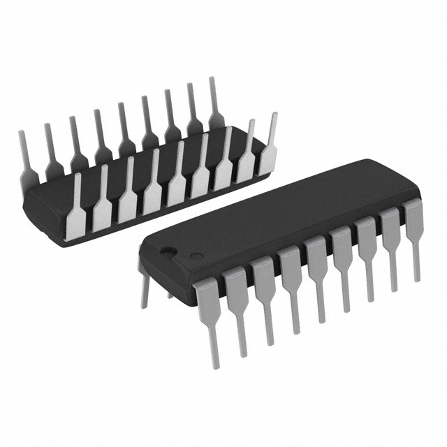
Available in 16-Pin Narrow SSOP Package
Single Supply 5V or ±5V Operation
Power Dissipation: 90mW (Typ)
Nap Mode with Instant Wake-Up: 15mW
Sleep Mode: 10mW
True Differential Inputs Reject Common Mode Noise
80MHz Full Power Bandwidth Sampling
Input Range (1mV/LSB): 0V to 4.096V or ±2.048V
Internal Reference Can Be Overdriven Externally
3-Wire Interface to DSPs and Processors (SPI and MICROWIRETM Compatible)Application Telecommunications
High Speed Data and Signal Acquisition
Digitally Multiplexed Data Acquisition Systems
Digital Radio Receivers
Spectrum Analysis
Low Power and Battery-Operated Systems
Handheld or Portable Instruments
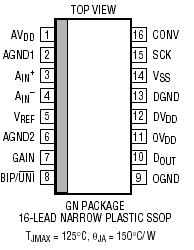
Imaging SystemsPinout SpecificationsAVDD = DVDD = OVDD = VDD (Notes 1, 2)
Supply Voltage (VDD) ................................................. 6V
Negative Supply Voltage (VSS) ............................... 6V
Total Supply Voltage (VDD to VSS) .......................... 12V
Analog Input Voltage
(Note 3) .......................... (VSS 0.3V) to (VDD + 0.3V)
Digital Input Voltage
(Note 4) .......................... (VSS 0.3V) to (VDD + 0.3V)
Digital Output Voltage ....... (VSS 0.3V) to (VDD + 0.3V)
Power Dissipation .............................................. 250mW
Operation Temperature Range
LTC1402C .............................................. 0°C to 70°C
LTC1402I............................................ 40°C to 85°C
Storage Temperature Range ................ 65°C to 150°C
Lead Temperature (Soldering, 10 sec).................. 300°CDescriptionThe LTC®1402 is a 12-bit, 2.2Msps sampling A/D converter. This high performance device includes a high dynamic range sample-and-hold and a precision reference. It operates from a single 5V supply or dual ±5V supplies and draws only 90mW from 5V.
The versatile differential input offers a unipolar range of 4.096V and a bipolar range of ±2.048V for dual supply systems where high performance op amps perform best, eliminating the need for special translation circuitry.
The high common mode rejection of LTC1402 allows users to eliminate ground loops and common mode noise by measuring signals differentially from the source.
Outstanding AC performance includes 72dB S/(N + D) and 93dB SFDR at the Nyquist input frequency of 1.1MHz with dual ±5V supplies and 84dB SFDR with a single 5V supply.
The LTC1402 has two power saving modes: Nap and Sleep. Nap mode consumes only 15mW of power and Sleep can wake up and convert immediately. In Sleep mode, it typically consumes 10mW of power. Upon powerup from Sleep mode, a reference ready (REFRDY) signal is available in the serial data word to indicate that the reference has settled and the chip is ready to convert.
The 3-wire serial port allows compact and efficient data transfer to a wide range of microprocessors, microcontrollers and DSPs. A digital output driver power supply pin allows direct connection to 3V or lower logic.

 LTC1402 Data Sheet


