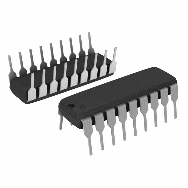
Features: Allows Lowest Drop 3.3V Supply SwitchingOperates on 3.3V or 5V Nominal Supplies3 Microamps Standby Current 80 Microamps ON CurrentDrives Low Cost N-Channel Power MOSFETs No External Charge Pump Components Controlled Switching ON and OFF TimesAvailable in 8-Pin SOICApplication Notebook C...
LTC1157: Features: Allows Lowest Drop 3.3V Supply SwitchingOperates on 3.3V or 5V Nominal Supplies3 Microamps Standby Current 80 Microamps ON CurrentDrives Low Cost N-Channel Power MOSFETs No External Charg...
SeekIC Buyer Protection PLUS - newly updated for 2013!
268 Transactions
All payment methods are secure and covered by SeekIC Buyer Protection PLUS.
Supply Voltage ........................................... 0.3V to 7V
Any Input Voltage ............. (VS + 0.3V) to (GND 0.3V)
Any Output Voltage ............. (VS + 12V) to (GND 0.3V)
Current (Any Pin)................................................. 50mA
Operating Temperature Range
LTC1157C............................................... 0°C to 70°C
Storage Temperature Range ................ 65°C to 150°C
Lead Temperature (Soldering, 10 sec)................. 300°C
DescriptionThe LTC1157 dual 3.3V micropower MOSFET gate driver makes it possible to switch either supply or ground reference loads through a low RDS(ON) N-channel switch (N-channel switches are required at 3.3V because Pchannel MOSFETs do not have guaranteed RDS(ON) with VGS £ 3.3V). The LTC1157 internal charge pump boosts the gate drive voltage 5.4V above the positive rail (8.7V above ground), fully enhancing a logic level N-channel switch for 3.3V high-side applications and a standard Nchannel switch for 3.3V low-side applications.
The gate drive voltage at 5V is typically 8.8V above supply (13.8V above ground), so standard N-channel MOSFET switches can be used for both high-side and low-side applications. Micropower operation, with 3mA standby current and 80mA operating current, makes the LTC1157 well suited for battery-powered applications. The LTC1157 is available in both 8-pin DIP and SOIC.