Features: Programmable Features
Unipolar/Bipolar Conversions
Differential/Single-Ended Multiplexer Configurations
Sample-and-Holds
Single Supply 5V, 10V or ±5V Operation
Direct 3- or 4-Wire Interface to Most MPU Serial Ports and All MPU Parallel I/O Ports
Analog Inputs Common Mode to Supply Rails
Resolution: 10 Bits
Total Unadjusted Error (A Grade): ±1LSB Over Temp
Fast Conversion Time: 20µs
Low Supply Current
LTC1091: 3.5mA Max, 1.5mA Typ
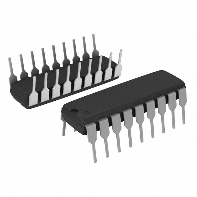
LTC1092/LTC1093/LTC1094: 2.5mA Max, 1mA TypPinout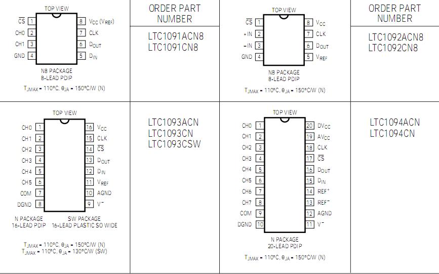 SpecificationsSupply Voltage (VCC) to GND or V .......................................... 12V
Negative Supply Voltage (V) ...................................... 6V to GND
Voltage
Analog Reference and LTC1091/2 CS
Inputs .............................................. (V) 0.3V to (VCC + 0.3V)
Digital Inputs (except LTC1091/2 CS) .................... 0.3V to 12V
Digital Outputs .......................................... 0.3V to (VCC + 0.3V)
Power Dissipation.................................................................. 500mW
Operating Temperature Range
LTC1091/2/3/4AC, LTC1091/2/3/4C.................... 40°C to 85°C
Storage Temperature Range ................................ 65°C to 150°C
Lead Temperature (Soldering, 10 sec.) ................................... 300°CDescriptionThe LTC
®1091/LTC1092/LTC1093/LTC1094 10-bit data acquisition systems are designed to provide complete function, excellent accuracy and ease of use when digitiz-ing analog data from a wide variety of signal sources and transducers. Built around a 10-bit, switched capacitor,successive approximation A/D core, these devices include software configurable analog multiplexers and bipolar and unipolar conversion modes as well as on-chip sample-and-holds. On-chip serial ports allow efficient data trans-fer to a wide range of microprocessors and microcontrol-lers. These circuits can provide a complete data acquisi-tion system in ratiometric applications or can be used withan external reference in others.
The high impedance analog inputs of LTC1093 and the ability to operate with reduced spans (below 1V full scale) allow direct connection to sensors and transducers in many applications, eliminating the need for gain stages.
An efficient serial port communicates without external hardware to most MPU serial ports and all MPU parallel I/O ports allowing eight channels of data to be transmitted over as few as three wires. This, coupled with low power consumption, makes remote location possible and facili-tates transmitting data through isolation barriers.
Temperature drift of offset, linearity and full-scale error of LTC1093 are all extremely low (1ppm/°C typically) allowing all grades to be specified with offset and linearity errors of ±0.5LSB maximum over temperature. In addition, the A grade devices are specified with full-scale error and total unadjusted error (including the effects of offset, linearity and full-scale errors) of ±1LSB maximum over tempera-ture. The lower grade has a full-scale specification of ±2LSB for applications where full scale is adjustable or less critical.

 LTC1093 Data Sheet