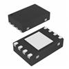
Features: 750MHz 3dB Small Signal Bandwidth 450MHz 3dB 2VP-P Large-Signal Bandwidth 120MHz ±0.1dB Bandwidth High Slew Rate: 2100V/s Fixed Gain of 1; No External Resistors Required 72dB Channel Separation at 10MHz 52dB Channel Separation at 100MHz 84dBc 2nd Harmonic Distortion at 10MHz, 2VP-P 87dB...
LT6556: Features: 750MHz 3dB Small Signal Bandwidth 450MHz 3dB 2VP-P Large-Signal Bandwidth 120MHz ±0.1dB Bandwidth High Slew Rate: 2100V/s Fixed Gain of 1; No External Resistors Required 72dB Channel Sepa...
SeekIC Buyer Protection PLUS - newly updated for 2013!
268 Transactions
All payment methods are secure and covered by SeekIC Buyer Protection PLUS.
Total Supply Voltage (V+ to V) ............................12.6V
Input Current (Note 2) ........................................±10mA
Output Current (Continuous) ..............................±70mA
⎯E⎯N to DGND Voltage (Note 2) .............................5.5V
SEL to DGND Voltage (Note 2) ....................................8V
Output Short-Circuit Duration (Note 3) .......... Indefi nite
Operating Temperature Range (Note 4) ...40 to 85
Specifi ed Temperature Range (Note 5) ....40 to 85
Junction Temperature
SSOP ................................................................ 150
QFN ................................................................... 125
Storage Temperature Range
SSOP ................................................. 65 to 150
QFN .................................................... 65 to 125
Soldering Temperature (10 sec) ........................ 300
Note 1: Absolute Maximum Ratings are those values beyond which the life of a device may be impaired.
Note 2: This parameter is guaranteed to meet specifi ed performance through design and characterization. It is not production tested.
Note 3: As long as output current and junction temperature are kept below the Absolute Maximum Ratings, no damage to the part will occur. Depending on the supply voltage, a heat sink may be required.
Note 4: The LT6556C is guaranteed functional over the operating temperature range of 40 to 85.
Note 5: The LT6556C is guaranteed to meet specifi ed performance from 0 to 70. The LT6556C is designed, characterized and expected to meet specifi ed performance from 40 and 85 but is not tested or QA sampled at these temperatures. The LT6556I is guaranteed to meet specifi ed performance from 40 to 85.
Note 6: In order to follow the constraints for 4.5V operation for PSRR and IPSRR testing at ± 2.25V, the DGND pin is set to V, the EN pin is set to V + 0.4V, and the SEL pin is set to either V + 0.4V or V + 4V. At ±6V and all other cases, DGND is set to ground and the EN and SEL pins are referenced from it.
The LT®6556 is a high speed triple 2:1 video multiplexer with an internally fi xed gain of 1. The individual buffers are optimized for performance with a 1k load and feature a 2VP-P 3dB bandwidth of 450MHz, making them ideal for driving very high resolution video signals. Separate power supply pins for each amplifi er boost channel separation to 72dB, allowing the LT6556 to excel in many high speed applications.
While the performance of the LT6556 is optimized for dual supply operation, it can also be operated with a single supply as low as 4.5V. Using dual 5V supplies, each amplifi er draws only 9.5mA. When disabled, the amplifi ers draw less than 330A and the outputs become high impedance. For applications requiring a fi xed gain of 2, refer to the LT6555 datasheet.
The LT6556 is available in 24-lead SSOP and ultra-compact 24-lead QFN packages.