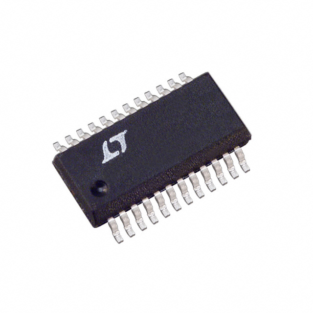
Features: `Optimized Image Rejection for 850MHz to 965MHz`High OIP3: +22.9dBm at 900MHz`Low Output Noise Floor at 5MHz Offset:No RF: 159.4dBm/HzPOUT = 4dBm: 153dBm/Hz`Integrated LO Buffer and LO Quadrature Phase Generator`50 AC-Coupled Single-Ended LO and RF Ports`50 DC Interface to Baseband Input...
LT5568-2: Features: `Optimized Image Rejection for 850MHz to 965MHz`High OIP3: +22.9dBm at 900MHz`Low Output Noise Floor at 5MHz Offset:No RF: 159.4dBm/HzPOUT = 4dBm: 153dBm/Hz`Integrated LO Buffer and LO Qua...
SeekIC Buyer Protection PLUS - newly updated for 2013!
268 Transactions
All payment methods are secure and covered by SeekIC Buyer Protection PLUS.
Supply Voltage .....................................................5.5V
Common Mode Level of BBPI, BBMI and
BBPQ, BBMQ .......................................................2.5V
Operating Ambient Temperature
(Note 2) ............................................... -40 to 85
Storage Temperature Range ............. -65 to 125
Voltage on Any Pin
Not to Exceed .................... -500mV to VCC + 500mV
CAUTION: This part is sensitive to ESD. It is very important that proper ESD precautions be observed when handling the LT5568-2.
Note 1: Stresses beyond those listed under Absolute Maximum Ratings may cause permanent damage to the device. Exposure to any Absolute Maximum Rating condition for extended periods may affect device reliability and lifetime.
Note 2: Specifi cations over the 40 to 85 temperature range are assured by design, characterization and correlation with statistical process controls.
The LT®5568-2 is a direct I/Q modulator designed for high performance wireless applications, including wireless infrastructure. It allows direct modulation of an RF signal using differential baseband I and Q signals. The LT5568-2 supports GSM, EDGE, CDMA, CDMA2000 and other systems that operate in the 850MHz to 965MHz band. It may be confi gured as an image reject upconverting mixer, by applying 90° phase-shifted signals to the I and Q inputs. The I/Q baseband inputs consist of voltage-to-current converters that in turn drive double-balanced mixers. The outputs of these mixers are summed and applied to an on-chip RF transformer, which converts the differential mixer signals to a 50 single-ended output. The four balanced I and Q baseband input ports are intended for DC coupling from a source with a common mode voltage level of about 0.5V. The LO path consists of an LO buffer with single-ended input, and precision quadrature generators that produce the LO drive for the mixers. The supply voltage range is 4.5V to 5.25V.