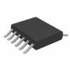
Features: Low Loss Replacement for ORing Diode Sourced Power Supplies External N-Channel MOSFETs for High Capability Internal Boost Regulator Supply for MOSFET Gate Drive Wide Input Range: 1.2V to 18V Fast Switching MOSFET Gate Control Input Under and Overvoltage Detection STATUS and FAULT Output...
LT4351: Features: Low Loss Replacement for ORing Diode Sourced Power Supplies External N-Channel MOSFETs for High Capability Internal Boost Regulator Supply for MOSFET Gate Drive Wide Input Range: 1.2V to ...
SeekIC Buyer Protection PLUS - newly updated for 2013!
268 Transactions
All payment methods are secure and covered by SeekIC Buyer Protection PLUS.
VIN Voltage ............................................... 0.3V to 19V
OUT Voltage ............................................ 0.3V to 19V
VDD Voltage ............................................. 0.3V to 30V
FAULT, STATUS Voltages ........................ 0.3V to 30V
FAULT, STATUS Current ........................................ 8mA
UV, OV Voltages ........................................ 0.3V to 9V
SW Voltage .............................................. 0.3V to 32V
Operating Temperature Range
LT4351C .................................................. 0°C to 70°C
LT4351I .............................................. 40°C to 85°C
Junction Temperature (Note 2) ............................ 125°C
Storage Temperature Range ................ 65°C to 150°C
Lead Temperature (Soldering, 10 sec).................. 300°C
The LT4351 creates a near-ideal diode using externalsingle or back-to-back N-channel MOSFETs. This ideal
diode function permits low loss ORing of multiple power sources. Power sources can easily be ORed together
increase total system power and reliability with minimal effect on supply voltage or efficiency. Disparate power
supplies can be efficiently ORed together.
The IC monitors the input supply with respect to the load and turns on the MOSFET(s) when the input supply
higher. If the MOSFET's RDS(ON) is sufficiently small, the LT4351 will regulate the voltage across the MOSFET(s)
15mV. A STATUS pin indicates the MOSFET on state. An internal boost regulator generates the MOSFET gate
drive voltage. Low operating voltage allows for OR'ing supplies as low as 1.2V.
The LT4351 will disable power passage during undervoltage or overvoltage conditions. These voltages are set
resistive dividers on the UV and OV pins. The undervoltage threshold has user programmable hysteresis. Overvoltage detection is filtered to reduce false triggering.
The LT4351 is available in a 10-pin MSOP.