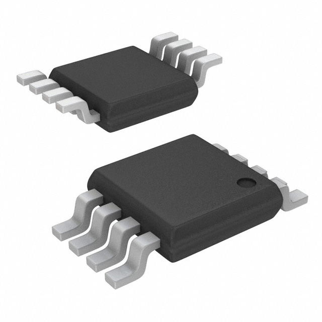
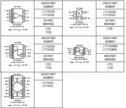
Features: 3.8nV/ÖHz Input Noise Voltage3.7mA Supply Current200MHz Gain BandwidthLow Total Harmonic Distortion: 85dBc at 1MHz70V/ms Slew Rate400mV Maximum Input Offset Voltage300nA Maximum Input Bias CurrentUnity-Gain StableCapacitive Load Stable Up to 100pF23mA Minimum Output CurrentSpecified...
LT1724: Features: 3.8nV/ÖHz Input Noise Voltage3.7mA Supply Current200MHz Gain BandwidthLow Total Harmonic Distortion: 85dBc at 1MHz70V/ms Slew Rate400mV Maximum Input Offset Voltage300nA Maximum Input...
SeekIC Buyer Protection PLUS - newly updated for 2013!
268 Transactions
All payment methods are secure and covered by SeekIC Buyer Protection PLUS.
Total Supply Voltage (V+ to V) ......................... .....12.6V
Input Voltage ............................................................. ±VS
Differential Input Voltage (Note 2) .......................... ±0.7V
Input Current (Note 2) .......................................... ±10mA
Output Short-Circuit Duration (Note 3) .............. Indefinite
Operating Temperature Range (Note 4)...40°C to 85°C
Specified Temperature Range (Note 5) ...40°C to 85°C
Maximum Junction Temperature ............................ 150°C
Storage Temperature Range ............... 65°C to 150°C
Lead Temperature (Soldering, 10 sec)................... 300°C
The LT®1722/LT1723/LT1724 are single/dual/quad, low noise, low power, high speed operational amplifiers. These products feature lower input offset voltage, lower input bias current and higher DC gain than devices with comparable bandwidth. The 200MHz gain bandwidth ensures high open-loop gain at video frequencies.
The low input noise voltage of LT1722/LT1723/LT1724 is achieved with reduced supply current. The total noise is optimized for a source resistance between 0.8k and 12k. Due to the input bias current cancellation technique used, the resistance seen by each input does not need to be balanced.