LS509_1235230

Features: • 140 mA typical current drain• low noise and distortion• 1.0 to 5 VDC operating range• independent preamplifier• 2 DC coupled stages• class A output stage• variable transducer current• Schottky diodes for MPO control• 4 kW microphone...

product image

LS509_1235230 Picture
SeekIC No. : 004399791 Detail

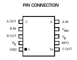
LS509_1235230: Features: • 140 mA typical current drain• low noise and distortion• 1.0 to 5 VDC operating range• independent preamplifier• 2 DC coupled stages• class A output st...

floor Price/Ceiling Price

Part Number:
LS509_1235230
Supply Ability:
5000

Price Break

  • Qty
  • 1~5000
  • Unit Price
  • Negotiable
  • Processing time
  • 15 Days
Total Cost: $ 0.00

SeekIC Buyer Protection PLUS - newly updated for 2013!

  • Escrow Protection.
  • Guaranteed refunds.
  • Secure payments.
  • Learn more >>

Month Sales

268 Transactions

Rating

evaluate  (4.8 stars)

Upload time: 2024/8/14

Payment Methods

All payment methods are secure and covered by SeekIC Buyer Protection PLUS.

Notice: When you place an order, your payment is made to SeekIC and not to your seller. SeekIC only pays the seller after confirming you have received your order. We will also never share your payment details with your seller.
Product Details

Description


Features:

• 140 mA typical current drain
• low noise and distortion
• 1.0 to 5 VDC operating range
• independent preamplifier
• 2 DC coupled stages
• class A output stage
• variable transducer current
• Schottky diodes for MPO control
• 4 kW microphone decoupling resistor


Pinout

  Connection Diagram


Specifications

Supply Voltage ...............................................5 V DC
Power Dissipation .........................................25 mW
Operating Temperature Range...... -10°C to 40° C
Storage Temperature Range......... -20°C to 70° C


Description

The LS509_1235230 is a Class A amplifier utilizing Gennum's proprietary low voltage JFET technology. It consists of two singleended, low noise inverting gain blocks, a Class A output stage, an on-chip microphone decoupling resistor and a pair of Schottky diodes for symmetrical peak clipping. Blocks A and B typically have an open loop voltage gain of 56 dB, with the closed loop gain set by the ratio of the feedback resistor to the source impedance. It is recommended that the maximum closed loop gain be 20 dB lower than the open loop gain. All blocks of the device are internally bias compensated, preventing any DC current flow via external feedback resistors. Without this compensation, audible scratchiness would be present during changes in volume control settings.

The output stage of the LS509_1235230 is a Class A current drive. It has a fixed reference voltage of typically 29 mV at pin 2 of the device. The current that flows in the transducer is the ratio of the 29 mV reference voltage and the on-chip emitter resistor (RE). To increase the bias current in the transducer, simply place an external RE resistor from pin 2 to ground, thereby decreasing the equivalent emitter resistance and increasing the current.

The LS509_1235230 also contains a pair of Schottky diodes in the feedback configuration of the output stage, which provides approximately 12 dB of MPO control. VB


Customers Who Bought This Item Also Bought

Margin,quality,low-cost products with low minimum orders. Secure your online payments with SeekIC Buyer Protection.
LED Products
Circuit Protection
Line Protection, Backups
Potentiometers, Variable Resistors
Sensors, Transducers
Connectors, Interconnects
View more