LP2981A-18DBVR

Features: Available in the Texas Instruments NanoStarTM Chip Scale PackageFixed/ADJ VersionsOutput Tolerance of: − 0.75% (A Grade) − 1.25% (Standard Grade)Ultra-Low Dropout, Typically − 200 mV at Full Load of 100 mA − 7 mV at 1 mAWide VIN Range ... 16 V MaxLow IQ ... 600 &m...

product image

LP2981A-18DBVR Picture
SeekIC No. : 004398703 Detail

LP2981A-18DBVR: Features: Available in the Texas Instruments NanoStarTM Chip Scale PackageFixed/ADJ VersionsOutput Tolerance of: − 0.75% (A Grade) − 1.25% (Standard Grade)Ultra-Low Dropout, Typically &#...

floor Price/Ceiling Price

Part Number:
LP2981A-18DBVR
Supply Ability:
5000

Price Break

  • Qty
  • 1~5000
  • Unit Price
  • Negotiable
  • Processing time
  • 15 Days
Total Cost: $ 0.00

SeekIC Buyer Protection PLUS - newly updated for 2013!

  • Escrow Protection.
  • Guaranteed refunds.
  • Secure payments.
  • Learn more >>

Month Sales

268 Transactions

Rating

evaluate  (4.8 stars)

Upload time: 2025/1/12

Payment Methods

All payment methods are secure and covered by SeekIC Buyer Protection PLUS.

Notice: When you place an order, your payment is made to SeekIC and not to your seller. SeekIC only pays the seller after confirming you have received your order. We will also never share your payment details with your seller.
Product Details

Description


Features:

Available in the Texas Instruments NanoStarTM Chip Scale Package
Fixed/ADJ Versions
Output Tolerance of:
   − 0.75% (A Grade)
   − 1.25% (Standard Grade)
Ultra-Low Dropout, Typically
   − 200 mV at Full Load of 100 mA
   − 7 mV at 1 mA
Wide VIN Range ... 16 V Max
Low IQ ... 600 µA Typ at Full Load of 100 mA
Shutdown Current... 0.01 µA Typ
Fast Transient Response to Line and Load
Overcurrent and Thermal Protection
High Peak Current Capability
Portable Applications
   − Mobile Phones
   − Laptops
   − Personal Digital Assistants (PDAs)
   − Digital Cameras and Camcorders
   − CD and MP3 Players


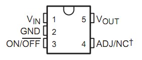
Pinout

  Connection Diagram


Specifications

Continuous input voltage range, VIN   . . . . . . . . . . . . . . . . . . . . . . . . . −0.3 V to 16 V
ON/OFF input voltage range, VON/OFF   . . . . . . . . . . . . . . . . . . . . . . . . −0.3 V to 16 V
Output voltage range (see Note 1)   . . . . . . . . . . . . . . . . . . . . . . . .. . . . −0.3 V to 9 V
Input/output voltage differential range, VIN-VOUT (see Note 2)   . . . . . −0.3 V to 16 V
Output current, IOUT (see Note 3)   . . . . . . .Internally limited (short-circuit protected)
Package thermal impedance, JA (see Notes 3 and 4): DBV package   .  . . . 206°C/W
                                                    YEQ/YZQ package   . . . . . . . . . . . . . . . . . . TBD°C/W
                                                  YEU/YZU package   . . . . . . . . . . . . . . . . . . . TBD°C/W
Operating virtual junction temperature, TJ  . . . . . . . . . . . . . . . . . . . . . . . . . . . .150°C
Storage temperature range, Tstg  . . . . . . . . . . . . . . . . . . . . . .. . . . . .−65°C to 150°C
† Stresses beyond those listed under "absolute maximum ratings" may cause permanent damage to the device. These are stress ratings only, and functional operation of the device at these or any other conditions beyond those indicated under "recommended operating conditions" is not implied. Exposure to absolute-maximum-rated conditions for extended periods may affect device reliability.
NOTES: 1. If load is returned to a negative power supply, the output must be diode clamped to GND.
2. The PNP pass transistor has a parasitic diode connected between the input and output. This diode normally is reverse biased (VIN > VOUT), but will be forward biased if the output voltage exceeds the input voltage by a diode drop (see Application Information for more details).
3. Maximum power dissipation is a function of TJ(max), JA, and TA. The maximum allowable power dissipation at any allowable ambient temperature is PD = (TJ(max) − TA)/JA. Operating at the absolute maximum TJ of 150°C can affect reliability.
4. The package thermal impedance is calculated in accordance with JESD 51-7.


Description

The LP2981A-18DBVR family of fixed-output, low-dropout regulators offers exceptional, cost-effective performance for both portable and nonportable applications. Available in adjustable version and in fixed voltages of 1.8 V, 2.5 V, 2.7 V, 2.8 V, 2.9 V, 3 V, 3.2 V, 3.3 V, 3.6 V, and 5 V, the family has an output tolerance of 0.75% for the A-grade devices (1.25% for the standard grade) and is capable of delivering 100-mA continuous load current. Standard regulator features, such as over-current and over-temperature protection, are included.

The LP2981A-18DBVR has features that make the regulator an ideal candidate for a variety of portable applications:

• Low dropout: A PNP pass element allows a typical dropout of 200 mV at 100-mA load current and 7 mV at 1-mA load.

• Low quiescent current: The use of a vertical PNP process allows for quiescent currents that are considerably lower than those associated with traditional lateral PNP regulators.

• Shutdown: A shutdown feature is available, allowing the regulator to consume only 0.01 µA when the ON/OFF pin is pulled low.

• Small packaging: For the most space-constraint needs, the regulator is available in SOT-23 package and NanoStarTM chip scale packaging. NanoStar package technology is a major breakthrough in IC packaging concepts, using the die as the package.


Customers Who Bought This Item Also Bought

Margin,quality,low-cost products with low minimum orders. Secure your online payments with SeekIC Buyer Protection.
Audio Products
Batteries, Chargers, Holders
Isolators
Undefined Category
Programmers, Development Systems
Prototyping Products
DE1
View more