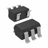
PinoutDescriptionThe LMV339I is designed as one kind of low-voltage (2.7V to 5.5V) versions of quad comparators. It is the most cost-effective solutions for applications where low voltage operation, low power, space saving, and price are the primary specifications in circuit design for portable co...
LMV339I: PinoutDescriptionThe LMV339I is designed as one kind of low-voltage (2.7V to 5.5V) versions of quad comparators. It is the most cost-effective solutions for applications where low voltage operation,...
SeekIC Buyer Protection PLUS - newly updated for 2013!
268 Transactions
All payment methods are secure and covered by SeekIC Buyer Protection PLUS.
The LMV339I is designed as one kind of low-voltage (2.7V to 5.5V) versions of quad comparators. It is the most cost-effective solutions for applications where low voltage operation, low power, space saving, and price are the primary specifications in circuit design for portable consumer products.
LMV339I has five features. (1)2.7V and 5V performance. (2)Low supply current which would be 170uA typ. (3)Input common-mode voltage range includes ground. (4)Low output saturation voltage is 200mV typ. (5)Open-collector output for maximum flexibility. Those are all the main features.
Some absolute maximum ratings of LMV339I have been concluded into several points as follow. (1)Its supply voltage Vcc would be 5.5V. (2)Its differential input voltage would be +/-5.5V. (3)Its input voltage range either input would be 0V to 5.5V. (4)Its package thermal impedance would be 206°C/W for DBV package and would be 252°C/W for DCK package. (5)Its operating virtual junction temperature would be 150°C. (6)Its storage temperature range would be from -65°C to 150°C. It should be noted that stresses above those listed in absolute maximum ratings may cause permanent damage to device.
Also some electrical characteristics of LMV339I at vcc+=2.7V are concluded as follow. (1)Its input offset voltage would be typ 1.7V and max 7V. (2)Its average temperature coefficient of input offset voltage would be typ 5uV/°C. (3)Its input bias current would be typ 10nA and max 250nA. (4)Its input offset current would be typ 5nA and max 50nA. (5)Its output current sinking would be min 5mA and typ 23mA. (6)Its output leakage current would be typ 0.003uA. (7)Its common mode input voltage range would be from -0.1V to 2V. (8)Its saturation voltage would be typ 200mV. (9)Its supply current would be typ 40uA and max 100uA. (10)Its propagation delay high to low level output switching would be typ 1000ns at input overdrive=10mV and would be typ 350ns for input overdrive=100mV. And so on. If you have any question or suggestion or want to know more information please contact us for details. Thank you!