Features: ·Multi-band cellular operation (example: GSM, PCN)·Support of GaAs HBT and bipolar technology·Shutdown mode for power save in Rx slot (0.15µA)·Integrated ramp filter·Built-in current source for biasing Schottky diodes·Pre-biasing of PA control gate voltage (VHOME)·GPRS compliant·Ex...
LMV248: Features: ·Multi-band cellular operation (example: GSM, PCN)·Support of GaAs HBT and bipolar technology·Shutdown mode for power save in Rx slot (0.15µA)·Integrated ramp filter·Built-in current...
SeekIC Buyer Protection PLUS - newly updated for 2013!
268 Transactions
All payment methods are secure and covered by SeekIC Buyer Protection PLUS.
·Multi-band cellular operation (example: GSM, PCN)
·Support of GaAs HBT and bipolar technology
·Shutdown mode for power save in Rx slot (0.15µA)
·Integrated ramp filter
·Built-in current source for biasing Schottky diodes
·Pre-biasing of PA control gate voltage (VHOME)
·GPRS compliant
·External loop compensation
·Detector diode temperature compensation
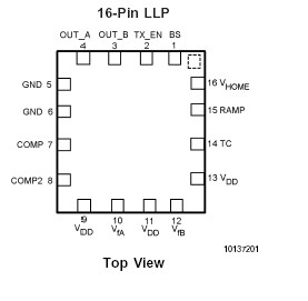
·Miniature packaging: LLP-16: 4mm x 4mm x 0.8mm
·GSM mobile phone
·TDMA RF control
·Wireless LAN
·PC and PDA modules
·GPS navigation modules
The LMV248 RF power amplifier controller allows simple implementation of transmit power control loops in GSM and DCS/PCS and mobile phones.
The LMV248 supports, GaAs HBT and bipolar RF power amplifiers.
The device operates from a single supply of 2.5V to 5V. The LMV248 includes an error amplifier with an input summing network, input and output band switches, input filters, and output drivers. Analog input signals processed are:
Coupler/detector voltages from GSM and PCN band power amplifier outputs.
Base band DAC ramp signal.
Temperature compensation diode voltages.
Pre-bias voltage for faster PA control. Selection of the GSM or PCN output driver is made using the GSM/PCN band select pin.
The On/OFF pin allows rapid power up or shutdown of the device during Tx or Rx slots. In the off mode, both output drivers are set low for PA shutdown. In the on mode, the non-active driver will remain low for continued PA shutdown. A single external capacitor/resistor combination is used to adjust the closed loop frequency response.
The LMV248 replaces multiple discrete parts, reducing board area and cost.
The LLP leadless package minimizes board footprint and permits flexible optimized PCB placement.