Features: VS = ±5V, TA = 25°C, RF = 1 KΩ, RG = 100Ω, RL = 100Ω, AV = AVMAX = 9.7V/V, Typical values unless specified.
`−3 dB BW 150 MHz
`Gain control BW 150 MHz
`Adjustment range (<10 MHz) 80 dB
`Output offset voltage ±55 mV
`Gain matching (limit) ±0.42 dB
`Supply voltage range 7V to 12V
`Slew rate (inverting) 1500 V/µs
`Supply Current (no load) 11 mA
`Linear Output Current ±60 mA
`Output Voltage Swing ±2.2V
`Input Noise Voltage 4.4 nV/Hz
`Input Noise Current 2.6 pA/Hz
`THD (20 MHz, RL = 100Ω, VO = 2 VPP) −45dBc
`Replacement for CLC5523
Application·Variable attenuator
·AGC
·Voltage controlled filter
·Video imaging processing
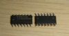
Pinout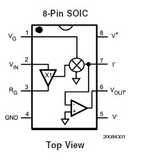 SpecificationsESD Tolerance (Note 4):
Human Body ...................................................................1000V
Machine Model ..................................................................100V
Input Current ...............................................................±10 mA
Output Current ...............................................120 mA (Note 3)
Supply Voltages (V+ - V−) ...............................................12.6V
Voltage at Input/ Output pins ...................V+ +0.8V, V− −0.8V
Storage Temperature Range .............................−65 to 150
Junction Temperature ......................................................150
Soldering Information:
Infrared or Convection (20 sec) .......................................235
Wave Soldering (10 sec) ..................................................260DescriptionThe LMH6504 is a wideband DC coupled voltage controlled gain stage followed by a high-speed current feedback Op Amp which can directly drive a low impedance load. Gain adjustment range is 80 dB for up to 10 MHz by varying the gain control input voltage, VG. Maximum gain is set by external components, and the gain can be reduced all the way to cut-off. Power consumption is 110 mW with a speed of 150 MHz and a gain control bandwidth (BW) of 150 MHz. Output referred DC offset voltage is less than 55 mV over the entire gain control voltage range. Device-to-device gain matching is within ±0.42 dB at maximum gain. Furthermore, gain is tested and guaranteed over a wide range.
The output current feedback Op Amp allows high frequency large signals (Slew Rate > 1500 V/µs) and can also drive a heavy load current (60 mA). Near ideal input characteristics (i.e. low input bias current, low offset, low pin 3 resistance) enable the device to be easily configured as an inverting amplifier as well (see Application Information section for details). To provide ease of use when working with a single supply, VG range is set to be from 0V to +2V relative to the ground pin potential (pin 4). VG input impedance is high in order to ease drive requirement. In single supply operation, the ground pin is tied to a "virtual" half supply. LMH6504 gain control is linear in dB for a large portion of the total gain control range. This makes the device suitable for AGC applications. For linear gain control applications, see LMH6503 data sheet.
The combination of minimal external components and small outline packages (SO8 and MSOP8) allows the LMH6504 to be used in space-constrained applications.

 LMH6504 Data Sheet