Features: VS = ±5V, TA = 25°C, RF = 1kΩ, RG = 174Ω, RL = 100Ω, AV
= AV(MAX) = 10, Typical values unless specified.
`-3dB BW 135MHz
`Gain control BW 100MHz
`Adjustment range (typical over temp) 70dB
`Gain matching (limit) ±0.7dB
`Slew rate 1800V/µs
`Supply current (no load) 37mA
`Linear output current ±75mA
`Output voltage (RL = 100Ω) ±3.2V
`Input voltage noise 6.6nV/Hz
`Input current noise 2.4pA/Hz
`THD (20MHz, RL = 100Ω, VO = 2VPP) −57dBc
`Replacement for CLC522Application·Variable attenuator
·AGC
·Voltage controller filter
· Multiplier
Pinout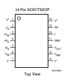 Specifications
| Gain Adjust Range |
70 dB |
| Analog Control BW |
100 MHz |
| Signal Channel BW |
135 MHz |
| Supply Min |
5 Volt |
| Supply Max |
12 Volt |
| Gain Control Interface |
Voltage |
| Slew Rate |
1800 Volts/usec |
| Supply Current |
37 mA |
| PowerWise Rating 2 |
274 uA/MHz |
| Output Current |
90 mA |
| Offset Voltage max, 25C |
370 mV |
| Max Input Bias Current |
20000 nA |
| Voltage Noise |
6.6 nV/root(Hz) |
| HD 2nd |
-60 dB |
| HD 3rd |
-61 dB |
| Diff Gain |
0.15 dB |
| Diff Phase |
0.22 % |
| Special Features |
Differential Input |
| Function |
VGA |
| Temperature Min |
-40 deg C |
| Temperature Max |
85 deg C |
| View Using Catalog |
ESD Tolerance: (Note 4)
Human Body .........................................................................2KV
Machine Model ....................................................................200V
Input Current ..................................................................±10mA
VIN Differential ..........................................................±(V+ −V−)
Output Current ..................................................120mA (Note 3)
Supply Voltages (V+ - V−) ..................................................12.6V
Voltage at Input/ Output pins .......................V+ +0.8V,V− - 0.8V
Soldering Information:
Infrared or Convection (20 sec) .........................................235
Wave Soldering (10 sec) ....................................................260
Storage Temperature Range .............................−65 to +150
Junction Temperature ......................................................+150DescriptionThe LMH6503 is a wideband DC coupled differential input voltage controlled gain stage followed by a high-speed current feedback Op Amp which can directly drive a low impedance load. Gain adjustment range is more than 70dB for up to 10MHz.
Maximum gain is set by external components and the gain can be reduced all the way to cut-off. Power consumption is 370mW with a speed of 135MHz . Output referred DC offset voltage is less than 350mV over the entire gain control voltage range. Device-to-device Gain matching is within 0.7dB at maximum gain. Furthermore, gain at any VG is tested and the tolerance is guaranteed. The output current feedback Op Amp allows high frequency large signals (Slew Rate = 1800V/µs) and can also drive heavy load current (75mA). Differential inputs allow common mode rejection in low level amplification or in applications where signals are carried over relatively long wires. For single ended operation, the unused input can easily be tied to ground (or to a virtual half-supply in single supply application). Inverting or non-inverting gains could be obtained by choosing one input polarity or the other.
To further increase versatility when used in a single supply application, gain control range is set to be from -1V to +1V relative to pin 11 potential (ground pin). In single supply operation, this ground pin is tied to a "virtual" half supply. Gain control pin has high input impedance to simplify its drive requirement. Gain control is linear in V/V throughout the gain adjustment range. Maximum gain can be set to be anywhere between 1V/V to 100V/V or higher. For linear in dB gain control applications, see LMH6502 datasheet.
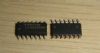
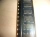
The LMH6503 is available in the SOIC-14 and TSSOP-14 package.
Reliability Metrics
| Part Number |
Process |
EFR Reject |
EFR Sample Size |
PPM |
LTA Rejects |
LTA Device Hours |
FITS |
MTTF (Hours) |
| LMH6503MA |
VIP 10 |
0 |
11856 |
0 |
0 |
1065000 |
4 |
302196657 |
| LMH6503MAX |
VIP 10 |
0 |
11856 |
0 |
0 |
1065000 |
4 |
302196657 |
| LMH6503MT |
VIP 10 |
0 |
11856 |
0 |
0 |
1065000 |
4 |
302196657 |
| LMH6503MTX |
VIP 10 |
0 |
11856 |
0 |
0 |
1065000 |
4 |
302196657 |
Note: The Early Failure Rates (EFR) were calculated as point estimate PPM based on rejects and sample size for EFR. The Long Term Failure Rates were calculated at 60% confidence using the Arrhenius equation at 0.7eV activation energy and derating the assumed stress temperature of 150°C to an application temperature of 55°C.For more information on Reliability Metrics, please click here.
Design Tools
| Title |
Size in Kbytes |
Date |
|
|
|
| CLC730033 SOIC-14 Evaluation Board - Included with LMH6503MA Sample Order |
325 Kbytes |
2-Feb-04 |
View Online |
Download |
|
If you have trouble printing or viewing PDF file(s), see Printing Problems.
|
More Application Notes
| Title |
Size in Kbytes |
Date |
|
| AN-1808: Application Note 1808 LMH730033 Evaluation Board |
683 Kbytes |
3-Mar-08 |
Download |
If you have trouble printing or viewing PDF file(s), see Printing Problems.
|

 LMH6503 Data Sheet