LMH6502

Features: VS = ±5V, TA = 25°C, RF = 1kΩ, RG = 174Ω, RL = 100Ω, AV = AV(MAX) = 10 Typical values unless specified.`-3dB BW 130MHz`Gain control BW 100MHz`Adjustment range (typical over temp) 70dB`Gain matching (limit) ±0.6dB`Slew rate 1800V/µs`Supply current (no load) 27mA`Li...

product image

LMH6502 Picture
SeekIC No. : 004396651 Detail

LMH6502: Features: VS = ±5V, TA = 25°C, RF = 1kΩ, RG = 174Ω, RL = 100Ω, AV = AV(MAX) = 10 Typical values unless specified.`-3dB BW 130MHz`Gain control BW 100MHz`Adjustment range (typical ov...

floor Price/Ceiling Price

Part Number:
LMH6502
Supply Ability:
5000

Price Break

  • Qty
  • 1~5000
  • Unit Price
  • Negotiable
  • Processing time
  • 15 Days
Total Cost: $ 0.00

SeekIC Buyer Protection PLUS - newly updated for 2013!

  • Escrow Protection.
  • Guaranteed refunds.
  • Secure payments.
  • Learn more >>

Month Sales

268 Transactions

Rating

evaluate  (4.8 stars)

Upload time: 2024/12/21

Payment Methods

All payment methods are secure and covered by SeekIC Buyer Protection PLUS.

Notice: When you place an order, your payment is made to SeekIC and not to your seller. SeekIC only pays the seller after confirming you have received your order. We will also never share your payment details with your seller.
Product Details

Description


Features:

VS = ±5V, TA = 25°C, RF = 1kΩ, RG = 174Ω, RL = 100Ω, AV = AV(MAX) = 10 Typical values unless specified.
`-3dB BW 130MHz
`Gain control BW 100MHz
`Adjustment range (typical over temp) 70dB
`Gain matching (limit) ±0.6dB
`Slew rate 1800V/µs
`Supply current (no load) 27mA
`Linear output current ±75mA
`Output voltage (RL = 100Ω) ±3.2V
`Input voltage noise 7.7nV/Hz
`Input current noise 2.4pA/Hz
`THD (20MHz, RL = 100Ω, VO = 2VPP) −53dBc
`Replacement for CLC520


Application

·Variable attenuator
·AGC
·Voltage controller filter
·Video imaging processing


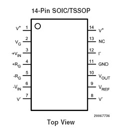
Pinout

  Connection Diagram


Specifications

ESD Tolerance (Note 4):
Human Body ...................................................................2KV
Machine Model ..............................................................200V
Input Current ...........................................................±10mA
VIN Differential ......................................................±(V+ -V)
Output Current ............................................120mA (Note 3)
Supply Voltages (V+ - V) ...........................................12.6V
Voltage at Input/ Output pins ................V+ +0.8V,V - 0.8V
Storage Temperature Range ......................−65 to +150
Junction Temperature ...............................................+150
Soldering Information:
Infrared or Convection (20 sec) ..................................235
Wave Soldering (10 sec) .............................................260


Description

The LMH6502 is a wideband DC coupled differential input voltage controlled gain stage followed by a high-speed current feedback Op Amp which can directly drive a low impedance load. Gain adjustment range is more than 70dB for up to 10MHz. Maximum gain is set by external components and the gain can be reduced all the way to cut-off. Power consumption is 300mW with a speed of 130MHz. Output referred DC offset voltage is less than 350mV over the entire gain control voltage range. Device-to-device Gain matching is within ±0.6dB at maximum gain. Furthermore, gain at any VG is tested and the tolerance is guaranteed.

The output current feedback Op Amp allows high frequency large signals (Slew Rate = 1800V/µs) and can also drive heavy load current 75mA). Differential inputs allow common mode rejection in low level amplification or in applications where signals are carried over relatively long wires. For single ended operation, the unused input can easily be tied to ground (or to a virtual half-supply in single supply application). Inverting or non-inverting gains could be obtained by choosing one input polarity or the other. To provide ease of use when working with a single supply, VG range is set to be from 0V to +2V relative to pin 11 potential (ground pin). In single supply operation, this ground pin is tied to a "virtual" half supply. LMH6502 gain control is linear in dB for a large portion of the total gain control range. This makes the device suitable for AGC circuits among other applications. For linear gain control applications, see the LMH6503 datasheet.

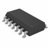
The LMH6502 is available in the SOIC-14 and TSSOP-14 package.


Customers Who Bought This Item Also Bought

Margin,quality,low-cost products with low minimum orders. Secure your online payments with SeekIC Buyer Protection.
Boxes, Enclosures, Racks
Crystals and Oscillators
LED Products
RF and RFID
Static Control, ESD, Clean Room Products
Optoelectronics
View more