Input Bias Current (Max)
:
Output Current
:
Number of Channels
: 1
Mounting Style
: SMD/SMT
Packaging
: Reel
Shutdown
: No
Common Mode Rejection Ratio (Min)
: 70 dB
Maximum Operating Temperature
: + 85 C
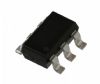
Package / Case
: SOT-23
Input Offset Voltage
: 6 mV at 5 V
Operating Supply Voltage
: 3 V, 5 V, 9 V, 12 V, 15 V, 18 V, 24 V, 28 V
Slew Rate
: 1.25 V/us at +/- 6 V
Pinout
 Description
The LM7301IM5 is designed as one kind of low power, 4MHz GBW, rail-to-rail input-output operational amlifiers in tinypak package which provides high performance in a wide range of applications. It offers greater than rail-to-rail input range, full rail-to-rail output swing, large capacitive load driving ability and low distortion.
LM7301IM5 has nine features. (1)Tiny SOT23-5 package saves space. (2)Greater than rail-to-rail input CMVR -0.25V to 5.25V. (3)Rail-to-rail output swing 0.07V to 4.93V. (4)Wide gain-bandwidth 4MHz. (5)Low supply current 0.6mA. (6)Wide supply range 1.8V to 32V. (7)High PSRR 104dB. (8)High CMRR 93dB. (9)Excellent gain 97dB. Those are all the main features.
Some absolute maximum ratings of LM7301IM5 have been concluded into several points as follow. (1)Its ESD tolerance would be 2500V. (2)Its differential input voltage would be 15V. (3)Its voltage at input/output pin would be (V+)+0.3V to (V-)-0.3V. (4)Its supply voltage would be 35V. (4)Its current at input pin would be +/-10mA. (5)Its current at output pin would be +/-20mA. (6)Its current at power supply pin would be 25mA. (7)Lead temperature soldering 10 seconds would be 260°C. (8)Its storage temperature range would be from -65°C to 150°C. (9)Its junction temperature would be 150°C. It should be noted that stresses above those listed in absolute maximum ratings may cause permanent damage to device.
Also some 5.0Vdc electrical characteristics of LM7301IM5 are concluded as follow. (1)Its input offset voltage would be typ 0.03mV and max 6mV. (2)Its input offset voltage average drift would be typ 2uV/°C. (3)Its input bias current would be typ 90nA and max 200nA. (4)Its input offset current would be typ 0.7nA and max 70nA. (5)Its input resistance would be typ 39Mohms. (6)Its common mode rejection ratio would be typ 88dB and min 70dB. (7)Its power supply rejection ratio would be typ 104dB and min 87dB. And so on. If you have any question or suggestion or want to know more information please contact us for details. Thank you!

 LM7301IM5 Data Sheet