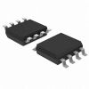
LM5112

Features: ·Compound CMOS and bipolar outputs reduce output current variation· 7A sink/3A source current· Fast propagation times (25 ns typical)·Fast rise and fall times (14 ns/12 ns rise/fall with 2 nF load)·Inverting and non-inverting inputs provide either configuration with a single device· Supp...

product image

LM5112 Picture
SeekIC No. : 004395971 Detail

LM5112: Features: ·Compound CMOS and bipolar outputs reduce output current variation· 7A sink/3A source current· Fast propagation times (25 ns typical)·Fast rise and fall times (14 ns/12 ns rise/fall with 2...

floor Price/Ceiling Price

Part Number:
LM5112
Supply Ability:
5000

Price Break

  • Qty
  • 1~5000
  • Unit Price
  • Negotiable
  • Processing time
  • 15 Days
Total Cost: $ 0.00

SeekIC Buyer Protection PLUS - newly updated for 2013!

  • Escrow Protection.
  • Guaranteed refunds.
  • Secure payments.
  • Learn more >>

Month Sales

268 Transactions

Rating

evaluate  (4.8 stars)

Upload time: 2024/6/12

Payment Methods

All payment methods are secure and covered by SeekIC Buyer Protection PLUS.

Notice: When you place an order, your payment is made to SeekIC and not to your seller. SeekIC only pays the seller after confirming you have received your order. We will also never share your payment details with your seller.
Product Details

Description


Features:

·Compound CMOS and bipolar outputs reduce output current variation
· 7A sink/3A source current
· Fast propagation times (25 ns typical)
·Fast rise and fall times (14 ns/12 ns rise/fall with 2 nF load)
·Inverting and non-inverting inputs provide either configuration with a single device
· Supply rail under-voltage lockout protection
· Dedicated input ground (IN_REF) for split supply or single supply operation
· Power Enhanced 6-pin LLP package (3.0mm x 3.0mm)
·Output swings from VCC to VEE which can be negative relative to input ground


Specifications

VCC to VEE ................................................................................−0.3V to 15V
VCC to IN_REF ..........................................................................−0.3V to 15V
IN/INB to IN_REF ......................................................................−0.3V to 15V
IN_REF to VEE ..............................................................................−0.3V to 5V
Storage Temperature Range ...........................................−55°C to +150°C
Maximum Junction Temperature .......................................................+150°C
Operating Junction Temperature ..........................................−40°C+125°C
ESD Rating ..............................................................................................2kV


Description

The LM5112 MOSFET gate driver provides high peak gate drive current in the tiny LLP-6 package (SOT23 equivalent footprint) with improved package power dissipation required for high frequency operation. The compound output driver stage includes MOS and bipolar transistors operating in parallel that together sink more than 7A peak from capacitive loads. Combining the unique characteristics of MOS and bipolar devices reduces drive current variation with voltage and temperature. Under-voltage lockout protection is provided to prevent damage to the MOSFET due to insufficient gate turn-on voltage. The LM5112 provides both inverting and non-inverting inputs to satisfy requirements for inverting and non-inverting gate drive with a single device type.


Customers Who Bought This Item Also Bought

Margin,quality,low-cost products with low minimum orders. Secure your online payments with SeekIC Buyer Protection.
Prototyping Products
DE1
Optical Inspection Equipment
Cables, Wires
Inductors, Coils, Chokes
View more