Features: ·Independently drives two N-Channel MOSFETs·Compound CMOS and bipolar outputs reduce output current variation· 5A sink/3A source current capability·Two channels can be connected in parallel to double the drive current·Independent inputs (TTL compatible)·Fast propagation times (25 ns typi...
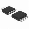
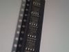
LM5110: Features: ·Independently drives two N-Channel MOSFETs·Compound CMOS and bipolar outputs reduce output current variation· 5A sink/3A source current capability·Two channels can be connected in paralle...
SeekIC Buyer Protection PLUS - newly updated for 2013!
268 Transactions
All payment methods are secure and covered by SeekIC Buyer Protection PLUS.
·Independently drives two N-Channel MOSFETs
·Compound CMOS and bipolar outputs reduce output current variation
· 5A sink/3A source current capability
·Two channels can be connected in parallel to double the drive current
·Independent inputs (TTL compatible)
·Fast propagation times (25 ns typical)
·Fast rise and fall times (14 ns/12 ns rise/fall with 2 nF load)
·Dedicated input ground pin (IN_REF) for split supply or single supply operation
· Outputs swing from VCC to VEE which can be negative relative to input ground
·Available in dual non-inverting, dual inverting and combination configurations
·Shutdown input provides low power mode
·Supply rail under-voltage lockout protection
· Pin-out compatible with industry standard gate drivers
· Synchronous Rectifier Gate Drivers
·Switch-mode Power Supply Gate Driver
·Solenoid and Motor Drivers
·Power Level Shifter
VCC to VEE ...............................................................................−0.3V to 15V
VCC to IN_REF .........................................................................−0.3V to 15V
IN to IN_REF, nSHDN to IN_REF ..............................................−0.3V to 15V
IN_REF to VEE ........................................................................... −0.3V to 5V
Storage Temperature Range, (TSTG) .............................−55°C to +150°C
Maximum Junction Temperature,
(TJ(max)) ........................................................................................+150°C
Operating Junction Temperature ....................................................+125°C
ESD Rating .............................................................................................2kV
The LM5110 Dual Gate Driver replaces industry standard gate drivers with improved peak output current and efficiency. Each "compound" output driver stage includes MOS and bipolar transistors operating in parallel that together sink more than 5A peak from capacitive loads. Combining the unique characteristics of MOS and bipolar devices reduces drive current variation with voltage and temperature. Separate input and output ground pins provide Negative Drive Capability allowing the user to drive MOSFET gates with positive and negative VGS voltages. The gate driver control inputs are referenced to a dedicated input ground (IN_REF).
The gate driver outputs swing from VCC to the output ground VEE which can be negative with respect to IN_REF. The ability to hold MOSFET gates off with a negative VGS voltage reduces losses when driving low threshold voltage MOSFETs often used as synchronous rectifiers. When driving with conventional positive only gate voltage, the IN_REF and VEE pins are connected together and referenced to a common ground. Under-voltage lockout protection and a shutdown input pin are also provided. The drivers can be operated in parallel with inputs and outputs connected to double the drive current capability. This device is available in the SOIC-8 and the thermally-enhanced LLP-10 packages.