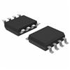
Pinout Specifications
| Function |
Master/Slave |
| Bits |
18 |
| Max PCLK Frequency |
30 MHz |
| VDDP |
1.6V to 2.0V |
| VDDI/O |
1.6V to 3.0V |
| Read/Write |
Yes |
| Target Application |
Mobile Phone |
| Recommended Interface |
CPU |
| Selectable Edge Rate |
Yes |
| PowerWise Technology |
Mobile Pixel Link Bridge |
| External Filters Req'd |
No |
| I/O Levels |
MPL-2 |
| Special Features |
Auto Power Down on Stop Clock , SPI Interface |
| ESD |
2 kV |
| View Using Catalog |
DescriptionThe LM4308 device adapts a 18-bit CPU style display interfaces to a MPL-2 SLVS differential serial link for displays. Two chip selects support a main and sub display up to and beyond 640 x 480 pixels. A mode pin configures the device as a Master (MST) or Slave (SLV). Both WRITE and READ operations are supported. CPU interface widths below 18-bits are supported by tieing unused inputs to a static level.
The differential line drivers and receivers conform to the JEDEC SLVS Standard. When noise is picked up as common-mode, it is rejected by the receivers. This is further enhanced with the 50 Ohm output impedance of the drivers. The 100 Ohm termination is integrated into the receivers.
Data integrity is insured with a 5-bit CRC field. CRC checking is done for both WRITE and READ operations. An Error (ERR) pin reports the occurrence of an error. A Write Only mode is also provided.
The interconnect is reduced from 23 signals to only 4 active signals with the LM4308 chipset easing flex interconnect design, size constraints and cost.
A low power sleep state entered when the PD* inputs are driven low.
The LM4308 device adapts a 18-bit CPU style display interfaces to a MPL-2 SLVS differential serial link for displays. Two chip selects support a main and sub display up to and beyond 640 x 480 pixels.
Features of the LM4308 are:(1)18-bit i80 CPU Display Interface;(2)supports up to 640 x 480 VGA formats;(3)differential SLVS interface;(4)dual displays supported;(5)WRITE and READ operations supported;(6)robust differential physical layer;(7)400mVpp differential signal swing;(8)internal 100 termination resistor;(9)low power consumption;(10)5-bit CRC for data integrity;(11)level translation between host and display;(12)low power sleep state;(13)3.3V tolerant master clock input regardless of VDDIO;(14)fast start up time - 1k CLK cycles;(15)1.6V to 2.0V core / analog supply voltage;(16)1.6V to 3.0V I/O supply voltage range.
The absolute maximum ratings of the LM4308 can be summarized as:(1):the parameter is supply voltage (VDDA),the rating is -0.3 to +2.2,the unit is V;(2):the parameter is supply voltage (VDD),the rating is -0.3 to +2.2,the unit is V;(3):the parameter is supply voltage (VDDIO),the rating is -0.3 to +3.6,the unit is V;(4):the parameter is LVCMOS input/output voltage,the rating is -0.3 to VDDIO+0.3,the unit is V;(5):the parameter is CLK LVCMOS input voltage,the rating is -0.3 to +3.3,the unit is V;(6):the parameter is SLVS input/output voltage,the rating is -0.3 to VDDA,the unit is V;(7):the parameter is junction temperature,the rating is +150,the unit is ;(8):the parameter is storage temperature,the rating is -65 to +150,the unit is .

 LM4308 Data Sheet


