LM1496H_1066411

Features: · Excellent carrier suppression 65 dB typical at 0.5 MHz50 dB typical at 10 MHz· Adjustable gain and signal handling· Fully balanced inputs and outputs· Low offset and drift· Wide frequency response up to 100 MHzPinoutSpecificationsIf Military/Aerospace specified devices are required,ple...

product image

LM1496H_1066411 Picture
SeekIC No. : 004394664 Detail

LM1496H_1066411: Features: · Excellent carrier suppression 65 dB typical at 0.5 MHz50 dB typical at 10 MHz· Adjustable gain and signal handling· Fully balanced inputs and outputs· Low offset and drift· Wide frequenc...

floor Price/Ceiling Price

Part Number:
LM1496H_1066411
Supply Ability:
5000

Price Break

  • Qty
  • 1~5000
  • Unit Price
  • Negotiable
  • Processing time
  • 15 Days
Total Cost: $ 0.00

SeekIC Buyer Protection PLUS - newly updated for 2013!

  • Escrow Protection.
  • Guaranteed refunds.
  • Secure payments.
  • Learn more >>

Month Sales

268 Transactions

Rating

evaluate  (4.8 stars)

Upload time: 2024/11/23

Payment Methods

All payment methods are secure and covered by SeekIC Buyer Protection PLUS.

Notice: When you place an order, your payment is made to SeekIC and not to your seller. SeekIC only pays the seller after confirming you have received your order. We will also never share your payment details with your seller.
Product Details

Description


Features:

· Excellent carrier suppression
    65 dB typical at 0.5 MHz
    50 dB typical at 10 MHz
· Adjustable gain and signal handling
· Fully balanced inputs and outputs
· Low offset and drift
· Wide frequency response up to 100 MHz


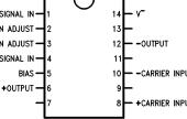
Pinout

  Connection Diagram


Specifications

If Military/Aerospace specified devices are required,please contact the National Semiconductor Sales ffice/Distributors for availability and specifications.
Internal Power Dissipation (Note 1)                             500 mW
Applied Voltage (Note 2)                                                     30V
Differential Input Signal (V7 - V8)                                    ±5.0V
Differential Input Signal (V4 - V1)                            ±(5+I5R0)V
Input Signal (V2 - V1,V3 - V4)                                              5.0V
Bias Current (I5)                                                               12mA
Operating Temperature Range LM1596              -55to +125
                                                 LM1496                   0 to a70
Storage Temperature Range                               -65to +150
Soldering Information
` Dual-In-Line Package
Soldering (10 seconds)                                                      260
` Small Outline Package
Vapor Phase (60 seconds)                                                 215
Infrared (15 seconds)                                                        220
See AN-450 ''Surface Mounting Methods and their effects on Product Reliability'' for other methods of soldering sur-face mount devices.


Description

The LM1596/LM1496H_1066411 are doubled balanced modulator-de- modulators which produce an output voltage proportional to the product of an input (signal) voltage and a switching (car- rier) signal. Typical applications include suppressed carrier modulation, amplitude modulation, synchronous detection, FM or PM detection, broadband frequency doubling and chopping.

The LM1496H_1066411 is specified for operation over the b55to a125 military temperature range. The LM1496 is speci-fied for operation over the 0to a70 temperature range.


Customers Who Bought This Item Also Bought

Margin,quality,low-cost products with low minimum orders. Secure your online payments with SeekIC Buyer Protection.
Isolators
RF and RFID
Potentiometers, Variable Resistors
Prototyping Products
DE1
Cables, Wires - Management
View more