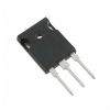
DescriptionThe LH2422 is designed as a CRT video driver which is a wide bandwidth, large signal amplifier to swing large voltages of short duration. It works on a transimpedance principle, in that about +/-6.5mA input current results in an output voltage of +/-20V. The primary application for this...
LH2422: DescriptionThe LH2422 is designed as a CRT video driver which is a wide bandwidth, large signal amplifier to swing large voltages of short duration. It works on a transimpedance principle, in that a...
SeekIC Buyer Protection PLUS - newly updated for 2013!
268 Transactions
All payment methods are secure and covered by SeekIC Buyer Protection PLUS.
The LH2422 is designed as a CRT video driver which is a wide bandwidth, large signal amplifier to swing large voltages of short duration. It works on a transimpedance principle, in that about +/-6.5mA input current results in an output voltage of +/-20V. The primary application for this very slewing amplifier is for driving high resolution monochrome or color graphics monitors. These drivers can easily energize a 10ns pixel.
The LH2422 has six features. (1)110MHz bandwidth at 40V swings. (2)Rise/fall times of 3.3ns. (3)Drives 8.5pF capacitive load. (4)Pin compatible with CR2424. (5)DC coupled for output level adjust. (6)Output signal can swing 50V. Those are all the main features.
Some absolute maximum ratings of LH2422 have been concluded into several points as follow. (1)Its supply voltage Vcc would be +70V. (2)Its power dissipation would be 7W. (3)Its storage temperature range would be from -40°C to 125°C. (4)Its operating temperature range would be from -20°C to 80°C. (5)Its lead temperature soldering <10 seconds would be 300°C. (6)Its ESD tolerance would be TBD. It should be noted that stresses above those listed in absolute maximum ratings may cause permanent damage to device.
Also some electrical characteristics of LH2422 are concluded as follow. (1)Its supply current would be min 39.5mA and typ 43.5mA and max 47.5mA. (2)Its input offset voltage would be min 1.15V and typ 1.55V and max 1.7V. (3)Its output offset voltage would be min 26V and typ 30V and max 34V. (4)Its power dissipation would be typ 5.3W and max 6W. (5)Its rise time would be typ 3.3ns and max 4ns. (6)Its fall time would be the same with the rise time. (8)Its low frequency tilt voltage would be typ 1.3V. (9)Its bandwidth would be min 100MHz and typ 110MHz. (10)Its insertion gain would be min 11.5V/V and typ 13V/V and max 14.5V/V. And so on. If you have any question or suggestion or want to know more information please contact us for details. Thank you!