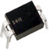
DescriptionThe LH1513AF is a kind of 100 output common driver LSI. The device is especially ideal for driving black and white LC panels used for palmtop personal computers because of its low-voltage operation (supply voltage for logic system: -5.5 to -2.5 V). When combined with the LH1514A segment driver, a low power consuming, high-precision LC panel display can be assembled. Data input/output pins are bidirectional, four data shift directions are pin-selectable.
There are some features of LH1513AF as follows: (1)supply voltage for the logic system: -5.5 to -2.5 V; (2)supply voltage for LC drive: -28.0 to -10.0 V (absolute maximum ratings -30.0 V); (3)number of LC driver outputs: 100; (4)low output impedance: 1.5 k (max); (5)shift clock frequency: 2.0 MHz (max); (6)low power consumption; (7)built-in 100-bits bidirectional shift register (divisible into 50-bits*2); (8)available in a single mode (100-bit shift register) or in a dual mode (50-bits shift register*2); (9)shift register circuit reset function when DISPOFF active; (10)supports high capacity LC panel display when combined with the LH1514A segment driver; (11)CMOS process (N-type silicon substrate).
The following is the absolute maximum ratings of LH1513AF: (1)supply voltage at VDD pin, VDD: -7.0 to +0.3 V when Ta=25, referenced to VSS; (2)supply voltage at V0L, V0R pins, V0: V5-0.3 to +0.3 V; (3)supply voltage at V1L, V1R pins, V1: V5-0.3 to +0.3 V; (4)supply voltage at V4L, V4R pins, V4: V5-0.3 to +0.3 V; (5)supply voltage at V5L, V5R pins, V5: -30.0 to +0.3 V; (6)input voltage at DIO1, DIO2, DMIN, SHLMODE, CK, FR, DISPOFF, VI: VDD-0.3 to +0.3 V; (7)storage temperature, Tstg: -45 to +125.

 LH1513AF Data Sheet


