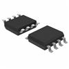
Pinout DescriptionThe LF355H is designed as one kind of JFET-input operational amplifiers which features several improvements compared to similar types from other manufactures: offset voltage drift with temperature and slw rate are guaranteed on all grades, not just on the more expensive A grad...
LF355H: Pinout DescriptionThe LF355H is designed as one kind of JFET-input operational amplifiers which features several improvements compared to similar types from other manufactures: offset voltage drift...
SeekIC Buyer Protection PLUS - newly updated for 2013!
268 Transactions
All payment methods are secure and covered by SeekIC Buyer Protection PLUS.
The LF355H is designed as one kind of JFET-input operational amplifiers which features several improvements compared to similar types from other manufactures: offset voltage drift with temperature and slw rate are guaranteed on all grades, not just on the more expensive "A" grades. Other specifications such as voltage gain and high temperature bias and offset currents are also improved.
LF355H has six features. (1)Guaranteed offset voltage drift on all grades. (2)Guaranteed slew rate on all grades. (3)Guaranteed low input offset current 10pA max. (4)Guaranteed low input bias current 50pA max. (5)Guaranteed high slew rate 10V/us min. (6)Fast settling to 0.01% 1.5us. Those are all the main features.
Some absolute maximum ratings of LF355H have been concluded into several points as follow. (1)Its supply voltage would be +/-17V. (2)Its differential input voltage would be +/-30V. (3)Its input voltage would be +/-16V. (4)Its output short circuit duration would be indefinite. (5)Its operating temperature range would be from 0°C to 70°C. (6)Its maximum junction temperature would be 100°C. (7)Its storage temperature range would be from -65°C to 150°C. (8)Its lead temperature soldering 10 seconds would be 300°C. It should be noted that stresses above those listed in absolute maximum ratings may cause permanent damage to device.
Also some electrical characteristics of LF355H are concluded as follow. (1)Its input offset voltage would be typ 3mV and max 8mV. (2)Its average TC of input offset voltage would be typ 5uV/°C and max 25uV/°C. (3)Its change in average TC with Vos adjust would be typ 0.5uV/°C per mV. (4)Its input offset current would be typ 3pA and max 50pA. (5)Its input bias current would be typ 30pA and max 200pA. (6)Its input resistance would be typ 10^12ohms. (7)Its large signal voltage gain would be typ 40V/mV and typ 200V/mV. And so on. If you have any question or suggestion or want to know more information please contact us for details. Thank you!