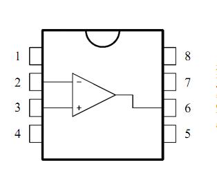
Features: `INTERNALLY ADJUSTABLE INPUT OFFSET VOLTAGE`LOWPOWER CONSUMPTION`WIDE COMMON-MODE (UP TO VCC+)AND`DIFFERENTIAL VOLTAGERANGE`LOWINPUT BIAS AND OFFSET CURRENT`OUTPUTSHORT-CIRCUIT PROTECTION`HIGH INPUT IMPEDANCE JFET INPUT STAGE`INTERNAL FREQUENCY COMPENSATION`LATCH UP FREE OPERATION`HIGH S...
LF251: Features: `INTERNALLY ADJUSTABLE INPUT OFFSET VOLTAGE`LOWPOWER CONSUMPTION`WIDE COMMON-MODE (UP TO VCC+)AND`DIFFERENTIAL VOLTAGERANGE`LOWINPUT BIAS AND OFFSET CURRENT`OUTPUTSHORT-CIRCUIT PROTECTION`...
SeekIC Buyer Protection PLUS - newly updated for 2013!
268 Transactions
All payment methods are secure and covered by SeekIC Buyer Protection PLUS.
Symbol | Parameter | Value | Unit |
VCC | Supply Voltage - (note 1) | ±18 | V |
Vi | Input Voltage - (note 3) | ±15 | V |
Vid | Differential Input Voltage - (note 2) | ±30 | V |
Ptot | Power Dissipation | 680 | mW |
Output Short-circuit Duration - (note 4) | Infinite | ||
Toper | Operating Free Air Temperature Range LF351 LF251 LF151 |
0to70 40 to 105 55 to 125 |
|
Tstg | Storage Temperature Range | 65 to 150 |
Notes : 1. All voltage values, except differential voltage, arewith respect to the zero reference level (ground) of the supply voltages where the
zero reference level is the midpoint between VCC+and VCC.
2. Differential voltages are at the non-inverting input terminalwith respect to the inverting input terminal.
3. The magnitude of the input voltage must never exceed the magnitude of the supply voltage or 15 volts, whichever is less.
4. The output may be shorted to ground or to either supply. Temperature and /or supply voltages must be limited to ensure that the dissipation rating is not exceeded.
These circuits LF251 are high speed JFET input single operationalamplifiers incorporatingwellmatched,high voltage JFET and bipolar transistors in a monolithic integrated circuit.
The LF251 feature high slew rates, low inputbiasand offset currents, and low offset voltage temperature coefficient.