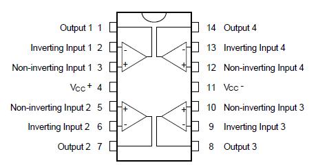
Features: ` LOW POWER CONSUMPTION
` WIDE COMMON-MODE (UP TO VCC+) AND DIFFERENTIAL VOLTAGE RANGE
` LOW INPUT BIAS AND OFFSET CURRENT
` OUTPUT SHORT-CIRCUIT PROTECTION
` HIGH INPUT IMPEDANCE JFET INPUT STAGE
` INTERNAL FREQUENCY COMPENSATION
` LATCH UP FREE OPERATION
` HIGH SLEW RATE : 16V/s (typ)Pinout Specifications
| Gain Bandwidth |
4 MHz |
| Channels |
4 Channels |
| Input OutputType |
Vcm to V+, Not R-R Out |
| Slew Rate |
13 Volts/usec |
| Supply Min |
5 Volt |
| Supply Max |
44 Volt |
| Offset Voltage max, 25C |
5 mV |
| Supply Current Per Channel |
1.8 mA |
| PowerWise Rating 2 |
450 uA/MHz |
| Max Input Bias Current |
10 nA |
| Output Current |
30 mA |
| Voltage Noise |
20 nV/root(Hz) |
| Shut down |
No |
| Special Features |
Undefined |
| Function |
Op Amp |
| Temperature Min |
-55 deg C |
| Temperature Max |
125 deg C |
| View Using Catalog |
|
Symbol |
Parameter |
LF147 |
LF247 |
LF347 |
Unit |
|
VCC |
Supply voltage - note 1) |
±18 |
V |
|
Vi |
Input Voltage - note 2) |
±15 |
V |
|
Vid |
Differential Input Voltage - note 3) |
±30 |
V |
|
Ptot |
Power Dissipation |
680 |
mW |
|
|
Output Short-circuit Duration - note 4) |
Infinite |
|
|
Toper |
Operating Free-air Temperature Range |
-55 to +125 |
-40 to +105 |
0 to +70 |
°C |
|
Tstg |
Storage Temperature Range |
-65 to +150 |
°C |
1.All voltage values, except differential voltage, are with respect to the zero reference level (ground) of the supply voltages where the zero reference level is the midpoint between VCC+ and VCC-.
2. The magnitude of the input voltage must never exceed the magnitude of the supply voltage or 15 volts, whichever is less.
3. Differential voltages are the non-inverting input terminal with respect to the inverting input terminal.
4. The output may be shorted to ground or to either supply. Temperature and/or supply voltages must be limited to ensure that the dissipation rating
is not exceeded
DescriptionThe LF147 is a low cost, high speed quad JFET input operational amplifier with an internally trimmed input offset voltage (BI-FET II™ technology). The device requires a low supply current and yet maintains a large gain bandwidth product and a fast slew rate. In addition, well matched high voltage JFET input devices provide very low input bias and offset currents. The LF147 is pin compatible with the standard LM148. This feature allows designers to immediately upgrade the overall performance of existing LF148 and LM124 designs.
The LF147 may be used in applications such as high speed integrators, fast D/A converters, sample-and-hold circuits and many other circuits requiring low input offset voltage, low input bias current, high input impedance, high slew rate and wide bandwidth. The device has low noise and offset voltage drift.
Reliability Metrics
| Part Number |
Process |
EFR Reject |
EFR Sample Size |
PPM |
LTA Rejects |
LTA Device Hours |
FITS |
MTTF (Hours) |
| LF147J |
BIFET |
0 |
12335 |
0 |
0 |
975000 |
4 |
276658912 |
Note: The Early Failure Rates (EFR) were calculated as point estimate PPM based on rejects and sample size for EFR. The Long Term Failure Rates were calculated at 60% confidence using the Arrhenius equation at 0.7eV activation energy and derating the assumed stress temperature of 150°C to an application temperature of 55°C.For more information on Reliability Metrics, please click here.
Design Tools
| Title |
Size in Kbytes |
Date |
|
|
|
| Amplifiers Selection Guide software for Windows |
8 Kbytes |
6-Mar-2007 |
View |
|
|
If you have trouble printing or viewing PDF file(s), see Printing Problems.
|

 LF147 Data Sheet


