LC75833JE

Features: • Supports both 1/3 duty 1/2 bias and 1/3 duty 1/3 biasLCD drive under serial data control.LC75833E, LC75833W: up to 105 segmentsLC75833JE: up to 93 segments(without the S12, S23, S24, S35 segment output pinsfrom the LC75833E, LC75833W)• Serial data input supports CCB format ...

product image

LC75833JE Picture
SeekIC No. : 004392137 Detail

LC75833JE: Features: • Supports both 1/3 duty 1/2 bias and 1/3 duty 1/3 biasLCD drive under serial data control.LC75833E, LC75833W: up to 105 segmentsLC75833JE: up to 93 segments(without the S12, S23, S2...

floor Price/Ceiling Price

Part Number:
LC75833JE
Supply Ability:
5000

Price Break

  • Qty
  • 1~5000
  • Unit Price
  • Negotiable
  • Processing time
  • 15 Days
Total Cost: $ 0.00

SeekIC Buyer Protection PLUS - newly updated for 2013!

  • Escrow Protection.
  • Guaranteed refunds.
  • Secure payments.
  • Learn more >>

Month Sales

268 Transactions

Rating

evaluate  (4.8 stars)

Upload time: 2024/5/28

Payment Methods

All payment methods are secure and covered by SeekIC Buyer Protection PLUS.

Notice: When you place an order, your payment is made to SeekIC and not to your seller. SeekIC only pays the seller after confirming you have received your order. We will also never share your payment details with your seller.
Product Details

Description


Features:

• Supports both 1/3 duty 1/2 bias and 1/3 duty 1/3 bias
LCD drive under serial data control.
LC75833E, LC75833W: up to 105 segments
LC75833JE: up to 93 segments
(without the S12, S23, S24, S35 segment output pins
from the LC75833E, LC75833W)
• Serial data input supports CCB format communication with the system controller.
• Serial data control of the power-saving mode based
backup function and all the segments forced off function
• Serial data control of switching between the segment
output port and the general-purpose output port functions
• High generality, since display data is displayed directly without decoder intervention.
• Independent VLCD for the LCD driver block (VLCD can be set to any
voltage in the range 2.7 to 6.0 volts, regardless of the logic block power-supply voltage.)
• The INH pin can force the display to the off state.
• RC oscillator circuit


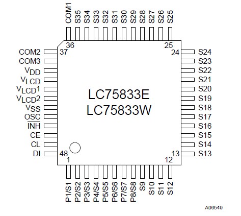
Pinout

  Connection Diagram


Specifications

Parameter

Symbol

Conditions

Ratings

Unit

Maximum supply voltage

VDD max

VDD

0.3 to +7.0

V

VLCD max

VLCD

0.3 to +7.0

V

Input voltage

VIN 1

CE, CL, DI, INH

0.3 to +7.0

V

VIN 2

OSC

0.3 to VDD + 0.3

V

VIN 3

VLCD 1, VLCD 2

0.3 to VLCD + 0.3

V

Output voltage

VOUT 1

OSC

0.3 to VDD + 0.3

V

VOUT 2

S1 to S35, COM1 to COM3, P1 to P8

0.3 to VLCD + 0.3

V

Output current

IOUT 1

S1 to S35

300

A

IOUT 2

COM1 to COM3

3

mA

IOUT 3

P1 to P8

5

mA

Allowable power dissipation

Pd max

Ta = 85°C

150

mW

Operating temperature

Topr

40 to +85

°C

Storage temperature

Tstg

55 to +125

°C


Customers Who Bought This Item Also Bought

Margin,quality,low-cost products with low minimum orders. Secure your online payments with SeekIC Buyer Protection.
Potentiometers, Variable Resistors
Programmers, Development Systems
Fans, Thermal Management
Sensors, Transducers
View more