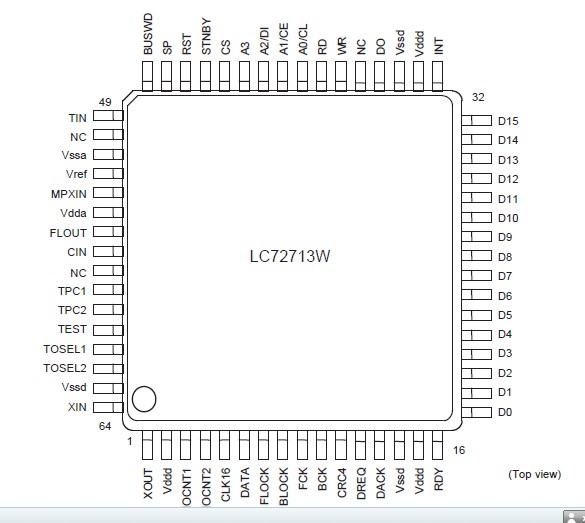
PinoutSpecifications Parameter Symbol Conditions Ratings Unit Maximum supply voltage VDD 0.3 to +7.0 V Input voltage VIN(1) A0/CL, A1/CE, A2/DI, RST, STNBY 0.3 to +7.0 V VIN(2) Pins other than VIN(1) 0.3 to VDD + 0.3 V Ou...
LC72713W: PinoutSpecifications Parameter Symbol Conditions Ratings Unit Maximum supply voltage VDD 0.3 to +7.0 V Input voltage VIN(1) A0/CL, A1/CE, A2/DI, RST, ...
SeekIC Buyer Protection PLUS - newly updated for 2013!
268 Transactions
All payment methods are secure and covered by SeekIC Buyer Protection PLUS.
Parameter |
Symbol |
Conditions |
Ratings |
Unit |
Maximum supply voltage |
VDD |
0.3 to +7.0 |
V | |
Input voltage |
VIN(1) |
A0/CL, A1/CE, A2/DI, RST, STNBY |
0.3 to +7.0 |
V |
VIN(2) |
Pins other than VIN(1) |
0.3 to VDD + 0.3 |
V | |
Output voltage |
VOUT(1) |
DO |
0.3 to +7.0 |
V |
VOUT(2) |
Pins other than VOUT(1) |
0.3 to VDD + 0.3 |
V | |
Output current |
IOUT(1) |
INT, RDY, DREQ, and D0 to D15 |
0 to 4.0 |
mA |
IOUT(2) |
Pins other than IOUT(1) |
0 to 2.0 |
mA | |
Allowable output current (total) |
ITTL |
Total for all the output pins |
20 |
mA |
Allowable power dissipation |
Pdmax |
Ta 85°C |
200 |
mW |
Operating temperature |
Topr |
40 to +85 |
°C | |
Storage temperature |
Tstg |
55 to +125 |
°C |
The LC72713W is data demodulator ICs for receiving FM multiplex broadcasts for mobile reception in the DARC format. This IC includes an on-chip bandpass filter for extracting the DARC signal from the FM baseband signal. It also integrates a decoder circuit that performs the VICS data processing on the same chip and can implement a compact, multifunction VICS reception system. The LC72713W is an improved version of the LC72710W that features circuit improvements that allow a single tuner to receive both the VICS data and the dGPS data supported by the earlier device. Note that a contract with VICS Center is required to evaluate this sample IC and to produce end products that support VICS.