LC72710W

Features: • Adjustment-free 76 kHz SCF bandpass filter• Built-in VICS decoder• MSK delay detection system based on a 1T delay.• Error correction function based on a 2T delay (in the MSK detection stage)• Digital PLL based clock regeneration function• Shift-regis...

product image

LC72710W Picture
SeekIC No. : 004391891 Detail

LC72710W: Features: • Adjustment-free 76 kHz SCF bandpass filter• Built-in VICS decoder• MSK delay detection system based on a 1T delay.• Error correction function based on a 2T delay ...

floor Price/Ceiling Price
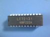
Part Number:
LC72710W
Supply Ability:
5000

Price Break

  • Qty
  • 1~5000
  • Unit Price
  • Negotiable
  • Processing time
  • 15 Days
Total Cost: $ 0.00

SeekIC Buyer Protection PLUS - newly updated for 2013!

  • Escrow Protection.
  • Guaranteed refunds.
  • Secure payments.
  • Learn more >>

Month Sales

268 Transactions

Rating

evaluate  (4.8 stars)

Upload time: 2024/5/28

Payment Methods

All payment methods are secure and covered by SeekIC Buyer Protection PLUS.

Notice: When you place an order, your payment is made to SeekIC and not to your seller. SeekIC only pays the seller after confirming you have received your order. We will also never share your payment details with your seller.
Product Details

Description


Features:

• Adjustment-free 76 kHz SCF bandpass filter
• Built-in VICS decoder
• MSK delay detection system based on a 1T delay.
• Error correction function based on a 2T delay (in the MSK detection stage)
• Digital PLL based clock regeneration function
• Shift-register 1T and 2T delay circuits
• Block and frame synchronization detection circuits
• Functions for setting the number of allowable BIC errors and the number of synchronization protection operations.
• Error correction using (272, 190) codes
• Built-in layer 4 CRC code checking circuit
• On-chip frame memory and memory control circuit for vertical correction


Specifications

Parameter Symbol Conditions Ratings Unit
Maximum supply voltage VDD max   (0.3 to +5.5)0.3 to +7.0 V
Input voltage VIN1 CL, CE, and DI pins 0.3 to +7.0 V
VIN2 Input pins other than VIN1 0.3 to VDD + 0.3 V
Output voltage VOUT1 DO 0 to 4.0 V
VOUT2 Output pins other than VOUT1 0 to 2.0 V
Output current IOUT BCLOCK, FCLOCK, and DO pins 20 mA
Allowable power dissipation Pd max Ta < 85°C 200 mW
Operating temperature Topg   40 to +85 °C
Storage temperature Tstg   45 to +125 °C


Customers Who Bought This Item Also Bought

Margin,quality,low-cost products with low minimum orders. Secure your online payments with SeekIC Buyer Protection.
Power Supplies - Board Mount
Boxes, Enclosures, Racks
Memory Cards, Modules
Isolators
Optical Inspection Equipment
Motors, Solenoids, Driver Boards/Modules
View more