LC723732

Features: • ROM- Up to 32K steps (32,767 ´ 16 bits)- The subroutine area holds 4 K steps (4,096 ´ 16 bits)• RAM- Up to 4 K ´ 4 bits (In banks 00 through 3F)LC723732 ROM: 32 KB, RAM 1 KBLC723740 ROM: 40 KB, RAM 2 KBLC723748 ROM: 48 KB, RAM 2 KBLC723756 ROM: 56 KB, ...

product image

LC723732 Picture
SeekIC No. : 004391872 Detail

LC723732: Features: • ROM- Up to 32K steps (32,767 ´ 16 bits)- The subroutine area holds 4 K steps (4,096 ´ 16 bits)• RAM- Up to 4 K ´ 4 bits (In banks 00 through 3F)LC723732 RO...

floor Price/Ceiling Price

Part Number:
LC723732
Supply Ability:
5000

Price Break

  • Qty
  • 1~5000
  • Unit Price
  • Negotiable
  • Processing time
  • 15 Days
Total Cost: $ 0.00

SeekIC Buyer Protection PLUS - newly updated for 2013!

  • Escrow Protection.
  • Guaranteed refunds.
  • Secure payments.
  • Learn more >>

Month Sales

268 Transactions

Rating

evaluate  (4.8 stars)

Upload time: 2024/5/28

Payment Methods

All payment methods are secure and covered by SeekIC Buyer Protection PLUS.

Notice: When you place an order, your payment is made to SeekIC and not to your seller. SeekIC only pays the seller after confirming you have received your order. We will also never share your payment details with your seller.
Product Details

Description


Features:

• ROM
- Up to 32K steps (32,767 ´ 16 bits)
- The subroutine area holds 4 K steps (4,096 ´ 16 bits)
• RAM
- Up to 4 K ´ 4 bits (In banks 00 through 3F)
LC723732 ROM: 32 KB, RAM 1 KB
LC723740 ROM: 40 KB, RAM 2 KB
LC723748 ROM: 48 KB, RAM 2 KB
LC723756 ROM: 56 KB, RAM 2 KB
LC723764 ROM: 64 KB, RAM 2 KB
• Stack
- 32 levels
• Serial I/O
- Three channels. These circuits can support both 2- wire and 3-wire 8-bit communication techniques, and can be switched between MSB first and LSB first operation.
- One of six internally generated serial transfer clock rates can be selected: 12.5, 37.5, 187.5, 281.25, 375, and 450 kHz.
• External interrupts
- Seven interrupt inputs (pins INT0 through INT5, and the HOLD pin)
These interrupts can be set to switch between rising and falling edges, although the HOLD pin only supports falling edge detection.
• Internal interrupts
- Seven interrupts; four internal timer interrupts, and three serial I/O interrupts.


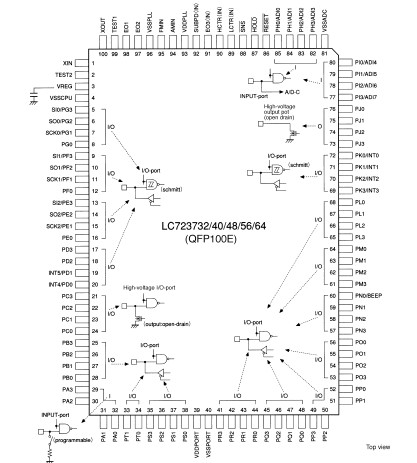
Pinout

  Connection Diagram


Specifications

Parameter Symbol Conditions Ratings Unit
Maximum supply voltage VDD max 0.3 to +6.5 V
put voltage VIN1 PC-PORT 0.3 to +15 V
VIN2 All input pins other than VIN1 0.3 to VDD + 0.3 V
Output voltage VOUT1 PC, PJ-PORT 0.3 to +15 V
VOUT2 All output pins other than VOUT1 0.3 to VDD + 0.3 V
Output current IOUT1 PC, PJ-PORT 0 to +5 mA
IOUT2 PB, PD, PE, PF, PG, PK, PL, PM, PN, PO, PP, PQ, PR,
PS, PT, PT-PORT, EO1, EO2, EO3, SUBPD
0 to +3 mA
Allowable power dissipation Pd max Ta = 40 to +85°C 400 mW
Operating temperature Topg 40 to +85 °C
Storage temperature Tstg 45 to +125 °C


Customers Who Bought This Item Also Bought

Margin,quality,low-cost products with low minimum orders. Secure your online payments with SeekIC Buyer Protection.
Integrated Circuits (ICs)
Industrial Controls, Meters
Programmers, Development Systems
Soldering, Desoldering, Rework Products
View more