LC7215

Features: PLL frequency synthesizer LSIs for MW and LW bands. .Reference frequencies of 1, 5, 9 and 10 kHz.On-chip transistor for the low-pass filter amplifier. Single output pin (CMOS output) . Controller clock output pin. Time-base output pin. All devices can be used for double conversion demodu...

product image

LC7215 Picture
SeekIC No. : 004391811 Detail

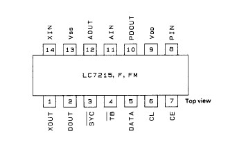
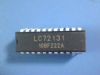
LC7215: Features: PLL frequency synthesizer LSIs for MW and LW bands. .Reference frequencies of 1, 5, 9 and 10 kHz.On-chip transistor for the low-pass filter amplifier. Single output pin (CMOS output) . Con...

floor Price/Ceiling Price

Part Number:
LC7215
Supply Ability:
5000

Price Break

  • Qty
  • 1~5000
  • Unit Price
  • Negotiable
  • Processing time
  • 15 Days
Total Cost: $ 0.00

SeekIC Buyer Protection PLUS - newly updated for 2013!

  • Escrow Protection.
  • Guaranteed refunds.
  • Secure payments.
  • Learn more >>

Month Sales

268 Transactions

Rating

evaluate  (4.8 stars)

Upload time: 2024/6/10

Payment Methods

All payment methods are secure and covered by SeekIC Buyer Protection PLUS.

Notice: When you place an order, your payment is made to SeekIC and not to your seller. SeekIC only pays the seller after confirming you have received your order. We will also never share your payment details with your seller.
Product Details

Description


Features:

PLL frequency synthesizer LSIs for MW and LW bands. .
Reference frequencies of 1, 5, 9 and 10 kHz.
On-chip transistor for the low-pass filter amplifier.
Single output pin (CMOS output) .
Controller clock output pin.
Time-base output pin.
All devices can be used for double conversion demodulation.
The LC7215F and 7215FM have expanded input frequency ranges.


Pinout

  Connection Diagram


Specifications

Parameter Symbol Conditions Ratings Unit
Maximum supply voltage VDD max VDD 0.3 to +6.5 V
Input voltage VIN1 All input pins 0.3 to VDD +0.3 V
VIN2 CE, CL, DATA (Note) 0.3 to +6.5 V
Output current IOUT AOUT 0 to 5 mA
Output voltage VOUT1 AOUT 0.3 to +15 V
VOUT2 SYC, TB 0.3 to +6.5 V
VOUT3 All output pins except VOUT1 and VOUT2 0.3 to VDD +0.3 V
Allowable power
dissipation

Pd max
Ta % 85°C 150 mW
Operating temperature Topr   40 to +85 °C
Storage temperature Tstg   55 to +125 V


Customers Who Bought This Item Also Bought

Margin,quality,low-cost products with low minimum orders. Secure your online payments with SeekIC Buyer Protection.
Boxes, Enclosures, Racks
Static Control, ESD, Clean Room Products
Motors, Solenoids, Driver Boards/Modules
Potentiometers, Variable Resistors
Hardware, Fasteners, Accessories
Industrial Controls, Meters
View more