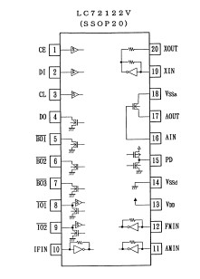
LC72122V

Features: • High-speed programmable frequency divider- FMIN: 10 to 250 MHz ..Pulse swallower divide-by-two prescaler built in)- AMIN: 2 to 40 MHz ......Pulse swallower 0.5 to 10 MHz ...Direct division• IF counter- IFIN: 0.4 to 12 MHz ......For use as an AM/FM IF counter• Referenc...

product image

LC72122V Picture
SeekIC No. : 004391787 Detail

LC72122V: Features: • High-speed programmable frequency divider- FMIN: 10 to 250 MHz ..Pulse swallower divide-by-two prescaler built in)- AMIN: 2 to 40 MHz ......Pulse swallower 0.5 to 10 MHz ...Direct ...

floor Price/Ceiling Price

Part Number:
LC72122V
Supply Ability:
5000

Price Break

  • Qty
  • 1~5000
  • Unit Price
  • Negotiable
  • Processing time
  • 15 Days
Total Cost: $ 0.00

SeekIC Buyer Protection PLUS - newly updated for 2013!

  • Escrow Protection.
  • Guaranteed refunds.
  • Secure payments.
  • Learn more >>

Month Sales

268 Transactions

Rating

evaluate  (4.8 stars)

Upload time: 2024/12/27

Payment Methods

All payment methods are secure and covered by SeekIC Buyer Protection PLUS.

Notice: When you place an order, your payment is made to SeekIC and not to your seller. SeekIC only pays the seller after confirming you have received your order. We will also never share your payment details with your seller.
Product Details

Description


Features:

• High-speed programmable frequency divider
- FMIN: 10 to 250 MHz ..Pulse swallower divide-by-two prescaler built in)
- AMIN: 2 to 40 MHz ......Pulse swallower 0.5 to 10 MHz ...Direct division
• IF counter
- IFIN: 0.4 to 12 MHz ......For use as an AM/FM IF counter
• Reference frequency
- Selectable from one of nine frequencies (crystal oscillator: 75 kHz) 1, 2.5, 3, 5, 3.125, 6.25, 12.5, 15, and 25 kHz
• Phase comparator
- Supports dead zone control
- Built-in unlock detection circuit
- Built-in deadlock clear circuit
- Sub-charge pump for fast frequency locking
• Built-in MOS transistor for forming an active low-pass filter
• I/O ports
- Dedicated output ports: 3
- I/O ports: 2
- Supports clock time base output


Pinout

  Connection Diagram


Specifications

Parameter Symbol Conditions Ratings Unit
Maximum supply voltage VDD max VDD V
Maximum input voltage VIN1 max CE, CL, DI V
VIN2max XIN, FMIN, AMIN, IFIN, AIN V
VIN3max IO1, IO2 V
Maximum output voltage VO1 max DO V
VO2 max XOUT, PD V
VO3 max BO1 to BO3,AOUT 0.3 to +15 V
VO4 max IO1, IO2 0.3 to +8 V
Maximum output current IO max BO1 to BO3, IO1, IO2, DO, AOUT 0 to 6.0 mA
Allowable power dissipation Pd max Ta ² 70°C: SSOP20 150 mW
Operating temperature Topr 20 to +70 °C
Storage temperature Tstg 40 to +125 °C


Customers Who Bought This Item Also Bought

Margin,quality,low-cost products with low minimum orders. Secure your online payments with SeekIC Buyer Protection.
Resistors
Prototyping Products
DE1
Cable Assemblies
Optoelectronics
Circuit Protection
Discrete Semiconductor Products
View more