LB1934T

Features: • Low voltage drive possible. When using same power supply for VCC and VS : VCC=VS=1.4V min. When using separate power supply for VCC and VS : VS=1.0V min., VCC=1.4V min.• Low saturation voltage : residual voltage (upper side transistor + lower side transistor) =0.5V typ. at ...

product image

LB1934T Picture
SeekIC No. : 004391197 Detail

LB1934T: Features: • Low voltage drive possible. When using same power supply for VCC and VS : VCC=VS=1.4V min. When using separate power supply for VCC and VS : VS=1.0V min., VCC=1.4V min.• Low ...

floor Price/Ceiling Price

Part Number:
LB1934T
Supply Ability:
5000

Price Break

  • Qty
  • 1~5000
  • Unit Price
  • Negotiable
  • Processing time
  • 15 Days
Total Cost: $ 0.00

SeekIC Buyer Protection PLUS - newly updated for 2013!

  • Escrow Protection.
  • Guaranteed refunds.
  • Secure payments.
  • Learn more >>

Month Sales

268 Transactions

Rating

evaluate  (4.8 stars)

Upload time: 2025/1/11

Payment Methods

All payment methods are secure and covered by SeekIC Buyer Protection PLUS.

Notice: When you place an order, your payment is made to SeekIC and not to your seller. SeekIC only pays the seller after confirming you have received your order. We will also never share your payment details with your seller.
Product Details

Description


Features:

• Low voltage drive possible. When using same power supply for VCC and VS : VCC=VS=1.4V min. When using separate power supply for VCC and VS : VS=1.0V min., VCC=1.4V min.
• Low saturation voltage : residual voltage (upper side transistor + lower side transistor) =0.5V typ. at Io=1A.
• Zero power dissipation in standby mode.
• Direct microcontroller drive possible (any strength relationships of voltage supported between microcontroller control signal and VCC or VS).
• Logic power supply and motor power supply can be supplied at separate pins.
• Built-in thermal protection circuit.
• Number of control signals can be optimized for the set. "2-motor control" or "1-motor + 2-load control" can be implemented by 3 control signals. In addition to the above, 4 control signals allow implemention of a "input ignore mode" where two control signals are used in conjunction with other IC input signals.
• Built-in spark killer diode.
• Compact, low-profile package (TSSOP-20 ; thickness=1.1 mm typ.)


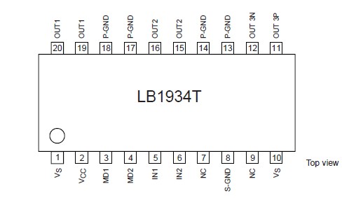
Pinout

  Connection Diagram


Specifications

Parameter Symbol Conditions Ratings Unit
Maximum input voltage VS max VS 0.3 to +8.0 V
VCC max VCC 0.3 to +8.0 V
Maximum output current IO max1 OUT1, OUT2 2000  
V
IO max2 OUT3P, OUT3N 1500 V
Maximum output voltage VO max OUT1, OUT2, OUT3P, OUT3N 0.3 to VS+VSF V
V
V
Maximum output current VI max MD1, MD2, IN1, IN2 0.3 to +8.0 mA
mA
mA
Allowable power dissipation Pd max With specified substrate* 850 mW
Operating temperature Topr   20 to +70 °C
Storage temperature Tstg   55 to +150 °C


Customers Who Bought This Item Also Bought

Margin,quality,low-cost products with low minimum orders. Secure your online payments with SeekIC Buyer Protection.
Optical Inspection Equipment
Soldering, Desoldering, Rework Products
Power Supplies - Board Mount
Undefined Category
Semiconductor Modules
Optoelectronics
View more