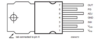
PinoutSpecifications Symbol Parameter Value Unit VPW, VSIG Supply Input Voltage 7 V ADJ pinPG and INH pins -0.3 to 40 to VSIG VV PTOT Power Dissipation @ Tamb = 50°CPower Dissipation @ Tcase = 90°C 215 WW Tst, Ti Storage Temperature -40 to +150 °CDescriptionTh...
L4956: PinoutSpecifications Symbol Parameter Value Unit VPW, VSIG Supply Input Voltage 7 V ADJ pinPG and INH pins -0.3 to 40 to VSIG VV PTOT Power Dissipation @ Tamb = 50°CPowe...
SeekIC Buyer Protection PLUS - newly updated for 2013!
268 Transactions
All payment methods are secure and covered by SeekIC Buyer Protection PLUS.
Symbol | Parameter | Value | Unit |
VPW, VSIG | Supply Input Voltage | 7 | V |
ADJ pin PG and INH pins |
-0.3 to 4 0 to VSIG |
V V | |
PTOT | Power Dissipation @ Tamb = 50°C Power Dissipation @ Tcase = 90°C |
2 15 |
W W |
Tst, Ti | Storage Temperature | -40 to +150 | °C |
The L4956 is an adjustable monolithic linear regulator designed to satisfy very heavy load transient and efficient power conversion from 3.3V to 1.26V and lower, up to 5A.
Designed in BCDII technology, L4956 uses a charge pump technique to have a proper internal N-channel gate drive. The signal supply voltage input VSIG can operate from 4.5V up to an absolute of7V and the power supply voltage input VPW can opearte from 3V min to an absolute of 7V. AnRDSON of 150mV gives a voltage drop of 750mV at 5A of load current.
Very fast load transients and ±1% of reference voltage precision makes L4956 Suitable for supplying last micrprocessors generation and low voltage logics.
The Heptawatt package enriches the device with auxiliary functions like power good and inhibit.