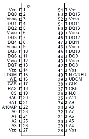
Features: • JEDEC standard 3.3V power supply
• LVTTL compatible with multiplexed address
• Four banks operation
• MRS cycle with address key programs
-. CAS latency (2 & 3)
-. Burst length (1, 2, 4, 8 & Full page)
-. Burst type (Sequential & Interleave)
• All inputs are sampled at the positive going edge of the system clock.
• Burst read single-bit write operation
• DQM for masking
• Auto & self refresh
• 64ms refresh period (4K cycle)
• Industrial Temperature Operation (- 40 to 85 °C)
Pinout Specifications
| Parameter |
Symbol |
Value |
Unit |
| Voltage on any pin relative to Vss |
VIN, VOUT |
-1.0 ~ 4.6 |
V |
| Voltage on VDD supply relative to Vss |
VDD ,VDDQ |
-1.0 ~ 4.6 |
V |
| Storage temperature |
TSTG |
-55 ~ +150 |
°C |
| Power dissipation |
PD |
1.0 |
W |
| Short circuit current |
IOS |
50 |
mA |
Note :
Permanent device damage may occur if ABSOLUTE MAXIMUM RATINGS are exceeded.
Functional operation should be restricted to recommended operating condition.
Exposure to higher than recommended voltage for extended periods of time could affect device reliability.
DescriptionThe K4S281632C is 134,217,728 bits synchronous high data rate Dynamic RAM organized as 4 x 2,097,152 words by 16 bits, fabricated with SAMSUNG¢s high performance CMOS technology. Synchronous design allows precise cycle control with the use of system clock I/O transactions are possible on every clock cycle. Range of operating frequencies, programmable burst length and programmable latencies allow the same device to be useful for a variety of high bandwidth, high performance memory system applications.

 K4S281632C-TI(P) Data Sheet


