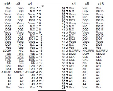
Features: • JEDEC standard 3.3V power supply• LVTTL compatible with multiplexed address• Four banks operation• MRS cycle with address key programs-. CAS latency (2 & 3)-. Burst length (1, 2, 4, 8 & Full page)-. Burst type (Sequential & Interleave)• All inp...
K4S280432F-TC(L)75: Features: • JEDEC standard 3.3V power supply• LVTTL compatible with multiplexed address• Four banks operation• MRS cycle with address key programs-. CAS latency (2 & 3)-....
SeekIC Buyer Protection PLUS - newly updated for 2013!
268 Transactions
All payment methods are secure and covered by SeekIC Buyer Protection PLUS.
Features: • JEDEC standard 3.3V power supply• LVTTL compatible with multiplexed addres...
Parameter | Symbol | Value | Unit |
Voltage on any pin relative to Vss | VIN, VOUT | -1.0 ~ 4.6 | V |
Voltage on VDD supply relative to Vss | VDD ,VDDQ | -1.0 ~ 4.6 | V |
Storage temperature | TSTG | -55 ~ +150 | °C |
Power dissipation | PD | 1.0 | W |
Short circuit current | IOS | 50 | mA |
Note :
Permanent device damage may occur if ABSOLUTE MAXIMUM RATINGS are exceeded.
Functional operation should be restricted to recommended operating condition.
Exposure to higher than recommended voltage for extended periods of time could affect device reliability.
The K4S280432F / K4S280832F / K4S281632F is 134,217,728 bits synchronous high data rate Dynamic RAM organized as 4 x8,388,608 words by 4 bits / 4 x 4,194,304 words by 8 bits / 4 x 2,097,152 words by 16 bits, fabricated with SAMSUNGs high performance CMOS technology. Synchronous design allows precise cycle control with the use of system clock I/O transactions are possible on every clock cycle. Range of operating frequencies, programmable burst length and programmable latencies allow the same device to be useful for a variety of high bandwidth, high performance memory system applications.