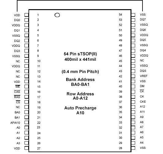
K4H510838B-NC_LA2

Features: • VDD : 2.5V ± 0.2V, VDDQ : 2.5V ± 0.2V for DDR266, 333• VDD : 2.6V ± 0.1V, VDDQ : 2.6V ± 0.1V for DDR400• Double-data-rate architecture; two data transfers per clock cycle• Bidirectional data strobe [DQS] (x4,x8)• Four banks operation• Differential cl...

product image

K4H510838B-NC_LA2 Picture
SeekIC No. : 004382784 Detail

K4H510838B-NC_LA2: Features: • VDD : 2.5V ± 0.2V, VDDQ : 2.5V ± 0.2V for DDR266, 333• VDD : 2.6V ± 0.1V, VDDQ : 2.6V ± 0.1V for DDR400• Double-data-rate architecture; two data transfers per clock cyc...

floor Price/Ceiling Price

Part Number:
K4H510838B-NC_LA2
Supply Ability:
5000

Price Break

  • Qty
  • 1~5000
  • Unit Price
  • Negotiable
  • Processing time
  • 15 Days
Total Cost: $ 0.00

SeekIC Buyer Protection PLUS - newly updated for 2013!

  • Escrow Protection.
  • Guaranteed refunds.
  • Secure payments.
  • Learn more >>

Month Sales

268 Transactions

Rating

evaluate  (4.8 stars)

Upload time: 2024/11/21

Payment Methods

All payment methods are secure and covered by SeekIC Buyer Protection PLUS.

Notice: When you place an order, your payment is made to SeekIC and not to your seller. SeekIC only pays the seller after confirming you have received your order. We will also never share your payment details with your seller.
Product Details

Description


Features:

• VDD : 2.5V ± 0.2V, VDDQ : 2.5V ± 0.2V for DDR266, 333
• VDD : 2.6V ± 0.1V, VDDQ : 2.6V ± 0.1V for DDR400
• Double-data-rate architecture; two data transfers per clock cycle
• Bidirectional data strobe [DQS] (x4,x8)
• Four banks operation
• Differential clock inputs(CK and CK)
• DLL aligns DQ and DQS transition with CK transition
• MRS cycle with address key programs
-. Read latency : DDR266(2, 2.5 Clock), DDR333(2.5 Clock), DDR400(3 Clock)
-. Burst length (2, 4, 8)
-. Burst type (sequential & interleave)
• All inputs except data & DM are sampled at the positive going edge of the system clock(CK)
• Data I/O transactions on both edges of data strobe
• Edge aligned data output, center aligned data input
• DM for write masking only (x4, x8)
• Auto & Self refresh
• 7.8us refresh interval(8K/64ms refresh)
• Maximum burst refresh cycle : 8
• 54pin sTSOP(II)-400 (Leaded & Pb-Free(RoHS compliant)) package


Pinout

  Connection Diagram


Specifications


Parameter
Value
SYMBOL
UNIT

Voltage on any pin relative to VSS
-0.5 ~ 3.6

V IN, VOUT

V
Voltage on VDD & VDDQ supply relative to VSS

-1.0 ~ 3.6
VDD, VDDQ
V

Storage temperature
-55 ~ +150
TSTG
Power dissipation
1.5
PD

W
Short circuit current
50
IOS

mA

Note : Permanent device damage may occur if ABSOLUTE MAXIMUM RATINGS are exceeded.
           Functional operation should be restricted to recommend operation condition.
           Exposure to higher than recommended voltage for extended periods of time could affect device reliability.


Description

The K4H510838B is 536,870,912 bits of double data rate synchronous DRAM organized as 4x 16,777,216 words by 8bits, fabricated with SAMSUNGs high performance CMOS technology. Synchronous features with Data Strobe allow extremely high performance 400Mb/s per pin. I/O transactions are possible on both edges of DQS. Range of operating frequencies, programmable burst length programmable latencies allow the device to be useful for a variety of high performance memory system applications. 9.0 General Description


Customers Who Bought This Item Also Bought

Margin,quality,low-cost products with low minimum orders. Secure your online payments with SeekIC Buyer Protection.
Cable Assemblies
Programmers, Development Systems
Isolators
Undefined Category
Power Supplies - Board Mount
View more