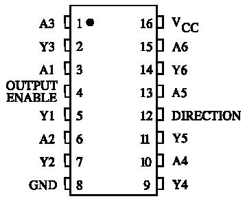
Features: • Operating Voltage Range: 3.0 to 18 V• Maximum input current of 1 µA at 18 V over full packagetemperature range; 100 nA at 18 V and 25°C• Noise margin (over full package temperature range): 1.0 V min @ 5.0 V supply 2.0 V min @ 10.0 V supply 2.5 V min @ 15.0 V sup...
IW4502B: Features: • Operating Voltage Range: 3.0 to 18 V• Maximum input current of 1 µA at 18 V over full packagetemperature range; 100 nA at 18 V and 25°C• Noise margin (over full p...
SeekIC Buyer Protection PLUS - newly updated for 2013!
268 Transactions
All payment methods are secure and covered by SeekIC Buyer Protection PLUS.
Symbol | Parameter | Value | Unit |
VCC | DC Supply Voltage (Referenced to GND) | -0.5 to +20 | V |
VIN | DC Input Voltage (Referenced to GND) | -0.5 to VCC +0.5 | V |
VOUT | DC Output Voltage (Referenced to GND) | -0.5 to VCC +0.5 | V |
IIN | DC Input Current, per Pin | ±10 | mA |
PD | Power Dissipation in Still Air, Plastic DIP+ SOIC Package+ |
750 500 |
mW |
Ptot | Power Dissipation per Output Transistor | 100 | mW |
Tstg | Storage Temperature | -65 to +150 | °C |
TL | Lead Temperature, 1 mm from Case for 10 Seconds (Plastic DIP or SOIC Package) |
260 | °C |
The IW4502B consists of six inverter/buffers with 3-state outputs. A logic "1" on the OUTPUT ENABLE input produces a high impedance state in all six outputs. This feature permits common busing of the outputs, thus simplifying system design. A logic "1" on the DIRECTION input switches all six outputs to logic "0" if the OUTPUT ENABLE input is a logic "0".