Features: • Integrates two high performance LDOs- VO1 - 300mA output- VO2 - 300mA output• Excellent transient response to large current steps• Excellent load regulation: <1% voltage change across full range of load current• High PSRR: 70dB @ 1kHz• Wide input voltag...
ISL9014: Features: • Integrates two high performance LDOs- VO1 - 300mA output- VO2 - 300mA output• Excellent transient response to large current steps• Excellent load regulation: <1% vol...
SeekIC Buyer Protection PLUS - newly updated for 2013!
268 Transactions
All payment methods are secure and covered by SeekIC Buyer Protection PLUS.
Supply Voltage (VIN) . . . . . . . . . . . . . . . . . . . . . . . . . . . . . . . +7.1V
All Other Pins . . . . . . . . . . . . . . . . . . . . . . . . . . . -0.3 to (VIN+0.3)V
Recommended Operating Conditions
Ambient Temperature Range (TA) . . . . . . . . .. . . . .-40°C to 85°C
Supply Voltage (VIN) . . . . . . . . . . . . . . . . . . . . . . . . . . 2.3V to 6.5V
Thermal Resistance (Notes 5, 6) JA (°C/W) JC (°C/W)
3x3 DFN Package . . . . . . .. . .. . .. . .. . .. . .. . . . . . . . . . . . 50 10
Junction Temperature Range . . . . . . . . . . . . . . . .-40°C to +125°C
Operating Temperature Range . . . . . .. . . . . . . . . .-40°C to +85°C
Storage Temperature Range . . . . . . . . . .. . . . . . .-65°C to +150°C
Maximum Lead Temperature (Soldering 10s) . . . . . . . . . . . +300°C
CAUTION: Stresses above those listed in "Absolute Maximum Ratings" may cause permanent damage to the device. This is a stress only rating and operation of the device at these or any other conditions above those indicated in the operational sections of this specification is not implied.
NOTES:
5. JA is measured in free air with the component mounted on a high effective thermal conductivity test board with "direct attach" features. See Tech Brief TB379.
6. JC, "case temperature" location is at the center of the exposed metal pad on the package underside. See Tech Brief TB379.
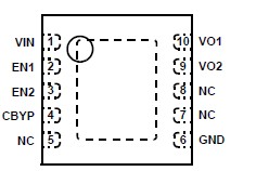
ISL9014 is a high performance dual LDO capable of sourcing 300mA current from both outputs. The dev ice has a low standby current and high-PSRR and is stable with output capacitance of 1F to 10F with ESR of up to 200m.
A reference bypass pin allows an external capacitor for adjusting a noise filter for low noise and high PSRR applications.
The quiescent current is typically only 45A with both LDOs enabled and active. Separate enable pins control each individual LDO output. When both enable pins are low, the device is in shutdown, typically drawing less than 0.1A.
Several combinations of voltage outputs are standard. Others are available on request. Output voltage options for each LDO range from 1.2V to 3.6V.