Features: • Integrated Multi-Phase Power Conversion
- 1, 2, or 3 Phase Operation
• Precision Output Voltage Regulation
- Differential Remote Voltage Sensing
- ±0.8% System Accuracy Over Temperature (for REF=0.6V and 0.9V)
- ±0.5% System Accuracy Over Temperature (for REF=1.2V and 1.5V)
- Usable for Output Voltages not Exceeding 2.3V
- Adjustable Reference-Voltage Offset
• Precision Channel Current Sharing
- Uses Loss-Less rDS(ON) Current Sampling
• Optional Load Line (Droop) Programming
- Uses Loss-Less Inductor DCR Current Sampling
• Variable Gate-Drive Bias - 5V to 12V
• Internal or External Reference Voltage Setting
- On-Chip Adjustable Fixed DAC Reference voltage with 2-bit Logic Input Selects from Four Fixed Reference Voltages (0.6V, 0.9V, 1.2V, 1.5V)
- Reference can be Changed Dynamically
- Can use an External Voltage Reference
• Overcurrent Protection
• Multi-tiered Overvoltage Protection
- OVP Pin to Drive Optional Crowbar Device
• Selectable Operation Frequency up to 1.5MHz per Phase
• Digital Soft-Start
• Capable of Start-up in a Pre-Biased Load
• Pb-Free Plus Anneal Available (RoHS Compliant)Application• High Current DDR/Chipset Core Voltage Regulators
• High Current, Low Voltage DC/DC Converters
• High Current, Low Voltage FPGA/ASIC DC/DC ConvertersPinout SpecificationsSupply Voltage, VCC . . . . . . . . . . . . . . . . . . . . . . . . . . . . -0.3V to +6V
Supply Voltage, PVCC. . . . . . . . . . . . . . . . . . . . . . . . . . . . -0.3V to +15V
Absolute Boot Voltage, VBOOT . . . . . . . . . . . . . . . . . . . . .GND - 0.3V to GND + 36V
Phase Voltage, VPHASE . . . . . . . . . . . . . . . . . . . . . . . . . . GND - 0.3V to 15V (PVCC = 12) GND - 8V (<400ns, 20J) to 24V (<200ns, VBOOT-PHASE = 12V)
Upper Gate Voltage, VUGATE . . . . . . . . . . . . . . . . . . . .. .VPHASE - 0.3V to VBOOT + 0.3V VPHASE - 3.5V (<100ns Pulse Width, 2J) to VBOOT + 0.3V
Lower Gate Voltage, VLGATE. . . . . . . . . . . . . . . . . . . . . . GND - 0.3V to PVCC + 0.3V GND - 5V (<100ns Pulse Width, 2J) to PVCC+ 0.3V
Input, Output, or I/O Voltage . . . . . . . . . . . . . . . . . . . . . GND - 0.3V to VCC + 0.3V
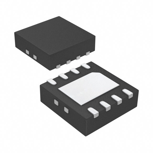
ESD Classification . . . . . . . . . . . . . . . . . . . . . . . . . . . . . .Class I JEDEC STDDescriptionThe ISL8103 is a three-phase PWM control IC with integrated MOSFET drivers. It provides a precision voltage regulation system for multiple applications including, but not limited to, high current low voltage point-of-load converters, embedded applications and other general purpose low voltage medium to high current applications.The integration of power MOSFET drivers into the controller IC marks a departure from the separate PWM controller and driver configuration of previous multi-phase product families. By reducing the number of external parts, this integration allows for a cost and space saving power management solution.
Output voltage can be programmed using the on-chip DAC or an external precision reference. A two bit code programs the DAC reference to one of 4 possible values (0.6V, 0.9V, 1.2V and 1.5V). A unity gain, differential amplifier is provided for remote voltage sensing, compensating for any potential difference between remote and local grounds. The output voltage can also be offset through the use of single external resistor. An optional droop function is also implemented and can be disabled for applications having less stringent output voltage variation requirements or experiencing less severe step loads.
A unique feature of the ISL8103 is the combined use of both DCR and r
DS(ON) current sensing. Load line voltage positioning and overcurrent protection are accomplished through continuous inductor DCR current sensing, while r
DS(ON) current sensing is used for accurate channel-current balance. Using both methods of current sampling utilizes the best advantages of each technique.
Protection features of this controller IC include a set of sophisticated overvoltage and overcurrent protection. Overvoltage results in the converter turning the lower MOSFETs ON to clamp the rising output voltage and protect the load. An OVP output is also provided to drive an optional crowbar device. The overcurrent protection level is set through a single external resistor. Other protection features include protection against an open circuit on the remote sensing inputs. Combined, these features provide advanced protection for the output load.

 ISL8103 Data Sheet


