ISL6612B

Features: Pin-to-pin Compatible with HIP6601 SOIC familyDual MOSFET Drives for Synchronous Rectified BridgeLow VCC Rising Threshold (7V) for IBA Applications.Advanced Adaptive Zero Shoot-Through ProtectionBody Diode DetectionAuto-zero of r Conduction Offset Effect DS(ON)Adjustable Gate Voltage (5V...

product image

ISL6612B Picture
SeekIC No. : 004380414 Detail

ISL6612B: Features: Pin-to-pin Compatible with HIP6601 SOIC familyDual MOSFET Drives for Synchronous Rectified BridgeLow VCC Rising Threshold (7V) for IBA Applications.Advanced Adaptive Zero Shoot-Through Pro...

floor Price/Ceiling Price

Part Number:
ISL6612B
Supply Ability:
5000

Price Break

  • Qty
  • 1~5000
  • Unit Price
  • Negotiable
  • Processing time
  • 15 Days
Total Cost: $ 0.00

SeekIC Buyer Protection PLUS - newly updated for 2013!

  • Escrow Protection.
  • Guaranteed refunds.
  • Secure payments.
  • Learn more >>

Month Sales

268 Transactions

Rating

evaluate  (4.8 stars)

Upload time: 2024/11/29

Payment Methods

All payment methods are secure and covered by SeekIC Buyer Protection PLUS.

Notice: When you place an order, your payment is made to SeekIC and not to your seller. SeekIC only pays the seller after confirming you have received your order. We will also never share your payment details with your seller.
Product Details

Description


Features:

Pin-to-pin Compatible with HIP6601 SOIC family
Dual MOSFET Drives for Synchronous Rectified Bridge
Low VCC Rising Threshold (7V) for IBA Applications.
Advanced Adaptive Zero Shoot-Through Protection
Body Diode Detection
Auto-zero of r Conduction Offset Effect DS(ON)
Adjustable Gate Voltage (5V to 12V) for Optimal Efficiency
36V Internal Bootstrap Schottky Diode
Bootstrap Capacitor Overcharging Prevention
Supports High Switching Frequency (up to 2MHz)
3A Sinking Current Capability
Fast Rise/Fall Times and Low Propagation Delays
Three-State PWM Input for Output Stage Shutdown
Three-State PWM Input Hysteresis for Applications With Power Sequencing Requirement
Pre-POR Overvoltage Protection
VCC Undervoltage Protection
Expandable Bottom Copper Pad for Enhanced Heat Sinking
Dual Flat No-Lead (DFN) Package
Near Chip-Scale Package Footprint; Improves PCB Efficiency and Thinner in Profile
Pb-Free Plus Anneal Available (RoHS Compliant)


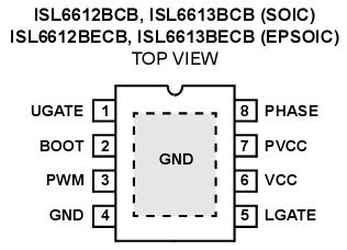
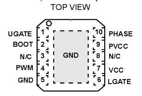
Pinout

  Connection Diagram  Connection Diagram


Specifications

Supply Voltage (VCC) . . . . . . . . . . . . . . . . . . . . . . . . . . . . . . . . .15V
Supply Voltage (PVCC) . . . . . . . . . . . . . . . . . . . . . . . . . .VCC + 0.3V
BOOT Voltage (VBOOT-GND ). . . . . . . . . . . . . . . . . . . . . . . . . . . 36V

Input Voltage (VPWM ) . . . . . . . . . . . . . . . . . . . . . GND - 0.3V to 7V
UGATE. . . . . . . . . . . . . . . . . . .... VPHASE - 0.3VDC to VBOOT+ 0.3V
VPHASE- 3.5V (<100ns Pulse Width, 2J) to VBOOT+ 0.3V
LGATE. . . . . . . . . . . . . . . . . . . . . .....GND - 0.3VDC to VPVCC+ 0.3V
GND - 5V (<100ns Pulse Width, 2J) to VPVCC + 0.3V
PHASE. . . . . . . . . . . . . . . . . . . . . . . . . . . GND - 0.3VDC....to 15VDC

GND - 8V (<400ns, 20J) to 30V (<200ns, VBOOT-GND<36V)
ESD Rating
Human Body Model . . . . . . . . . . . . . . . . . . ....... .Class I JEDEC STD


Description

The ISL6612B and ISL6613B are high frequency MOSFET drivers specifically designed to drive upper and lower power N-Channel MOSFETs in a synchronous rectified buck converter topology. These drivers combined with HIP63xx or ISL65xx Multi-Phase Buck PWM controllers and N-Channel MOSFETs form complete core-voltage regulator solutions for advanced microprocessors. The ISL6612B drives the upper gate to above rising VCC POR (7V), while the lower gate can be independently driven over a range from 5V to 12V. The ISL6613B drives both upper and lower gates over a range of 5V to 12V. This drivevoltage provides the flexibility necessary to optimize applications involving trade-offs between gate charge and conduction losses. These drivers are optimized for POL DC/DC Converters for IBA Systems. An advanced adaptive zero shoot-through protection is integrated to prevent both the upper and lower MOSFETs from conducting simultaneously and to minimize the dead time. These products add an overvoltage protection feature operational before VCC exceeds its turn-on threshold, at which the PHASE node is connected to the gate of the low side MOSFET (LGATE). The output voltage of the converter is then limited by the threshold of the low side MOSFET, which provides some protection to the microprocessor if the upper MOSFET(s) is shorted during initial start-up. These drivers also feature a three-state PWM input which, working together with Intersils multi-phase PWM controllers, prevents a negative transient on the output voltage when the output is shut down. This feature eliminates the Schottky diode that is used in some systems for protecting the load from reversed output voltage events.


Customers Who Bought This Item Also Bought

Margin,quality,low-cost products with low minimum orders. Secure your online payments with SeekIC Buyer Protection.
Audio Products
Memory Cards, Modules
Prototyping Products
DE1
Transformers
Inductors, Coils, Chokes
View more