Description
Features:
• Low Driver Output Resistance
-ROUT Maximum: ISL55100A 7.0Ω
• 18V I/O Range
• 50MHz Operation
• 4 Channel Driver/Receiver Pairs with Per Pin Flexibility
• Dual Level - Per Pin - Input Thresholds
• Differential or Single Ended Digital Inputs
• User Defined Comparator Output Levels
• Low Channel to Channel Timing Skew
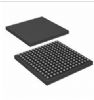
• Small Footprint (72 Ld QFN)
• Pb-Free Plus Anneal Available (RoHS Compliant)
Application
• Burn In ATE
• Wafer Level Flash Memory Test
• LCD Panel Test
• Low Cost ATE
• Instrumentation
• Emulation
• Device Programmers
Specifications
VCC to VEE . . . . . . . . . . . . . . . . . . . . . . . . . . . . . . . . . -0.5V to 19V
VEXT to VEE . . . . . . . . . . . . . . . . . . . . . . . . . . . . . . . . . -0.5V to 7V
Input Voltages
DATA, DRV EN, CVX, VH, VL, VINP, COMPX, LOSWING
. . . . . . . . . . . . . . . . . . . . . . . . . . . . .. . . .(VEE -0.5V) to (VCC +0.5V)
Output Voltages
DOUT . . . . . . . . . . . . . . . . . . . . . . . . . . .. . . . . (VL -0.5V) to (VH +0.5V)
QX . . . . . . . . . . . . .. . . . . .(COMP LOW -0.5V) to (COMP HIGH +0.5V)
Description
The ISL55100A is a Quad pin driver and window comparator fabricated in a wide voltage CMOS process. It is designed specifically for Test During Burn In (TDBI) applications, where cost, functional density, and power are all at a premium. This IC incorporates four channels of programmable drivers and window comparators into a small 72 Ld QFN package. Each channel has independent driver levels, data, and high impedance control. Each receiver has dual comparators which provide high and low threshold levels. The ISL55100A uses differential mode digital inputs, and can therefore mate directly with LVDS or CML outputs. Single ended logic families are handled by connecting one of the digital input pins to an appropriate threshold voltage (e.g., 1.4V for TTL compatibility). The comparator outputs are single-ended, and the output levels are user defined to mate directly with any digital technology. The 18V driver output and receiver input ranges allow this device to interface directly with TTL, ECL, CMOS (3V, 5V, and 7V), LVCMOS, and custom level circuitry, as well as the high voltage (Super Voltage) level required for many special test modes for Flash Devices.

 ISL55100A Data Sheet