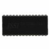
Features: • Access times of 70 and 85 ns• CMOS low power operation: - 120 mW (typical) operating - 6 µW (typical) standby• Low data retention voltage: 2V (min.)• Output Enable (OE) and two Chip Enable (CE1 and CE2) inputs for ease in applications• TTL compatible...
IS62LV2568LL: Features: • Access times of 70 and 85 ns• CMOS low power operation: - 120 mW (typical) operating - 6 µW (typical) standby• Low data retention voltage: 2V (min.)• Output...
SeekIC Buyer Protection PLUS - newly updated for 2013!
268 Transactions
All payment methods are secure and covered by SeekIC Buyer Protection PLUS.
Symbol | Parameter | Value | Unit |
VTERM | Terminal Voltage with Respect to GND | 0.5 to Vcc + 0.5 | V |
VCC | Vcc related to GND | 0.3 to +4.6 | V |
TBIAS | Temperature Under Bias | 40 to +85 | °C |
TSTG | Storage Temperature | 65 to +150 | °C |
PT | Power Dissipation | 0.7 | W |
Stress greater than those listed under ABSOLUTE MAXIMUM RATINGS may cause permanent damage to the device. This is a stress rating only and functional operation of the device at these or any other conditions above those indicated in the operational sections of this specification is not implied. Exposure to absolute maximum rating conditions for extended periods may affect reliability.
The ISSI IS62LV2568LL is a low voltage, 262,144 words by 8 bits, CMOS SRAM. IS62LV2568LL is fabricated using ISSI's low
voltage, six transistor (6T), CMOS technology. The IS62LV2568LL is targeted to satisfy the demands of the state-of-the-art
technologies such as cell phones and pagers.
When CE is HIGH (deselected), the IS62LV2568LL assumes a standby mode at which the power dissipation can be reduced down with CMOS input levels. Additionally, easy memory expansion is provided by using Chip Enable and Output Enable inputs, CE and OE. The active LOW Write Enable (WE) controls both writing and reading of the memory.
The IS62LV2568LL is available in 32-pin TSOP (Type I), STSOP (Type I), and 36-pin mini BGA.