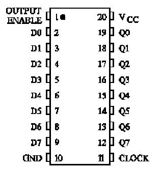
Features: · Output voltage levels are compatible with input levels of CMOS, NMOS and TTL ICS· Supply voltage range: 1.0 to 5.5 V· Low input current: 1.0 mÀ; 0.1 mÀ at Ò = 25 °Ñ· High Noise Immunity Characteristic of CMOS DevicesPinoutSpecifications Symbol Paramete...
IN74LV574: Features: · Output voltage levels are compatible with input levels of CMOS, NMOS and TTL ICS· Supply voltage range: 1.0 to 5.5 V· Low input current: 1.0 mÀ; 0.1 mÀ at Ò = 25 °&N...
SeekIC Buyer Protection PLUS - newly updated for 2013!
268 Transactions
All payment methods are secure and covered by SeekIC Buyer Protection PLUS.
Symbol | Parameter | Value | Unit |
VCC | DC Supply Voltage (Referenced to GND) | -0.5 to +7.0 | V |
IIK*1 | DC input diode current | ±20 | V |
IOK*2 | DC output diode current | ±50 | mA |
IO*3 | DC Output source or sink current | ±35 | mA |
ICC | DC VCC current | ±70 | mA |
IGND | DC GND current | ±70 | mA |
PD | Power dissipation per package: *4 Plastic DIP SO |
750 500 |
mW |
Tstg | Storage Temperature | -65 to +150 | °C |
TL | Lead Temperature, 1.5 mm (Plastic DIP Package), 0.3 mm (SO Package) from Case for 4 Seconds |
260 | °C |
The IN74LV574 is a low-voltage Si-gate CMOS device and is pin and function compatible with 74HC/HCT574.
The IN74LV574 is an octal D-type flipflop featuring separate D-type inputs for each flip-flop and non-inverting 3-state outputs for oriented applications. A clock (CP) and an outputenable (OE) input are common to all flip-flops. The eight flip-flops will store the state of their individual D-inputs that meet the set-up and hold times requirements on the LOWto-HIGH CP transition. When OE is LOW, the contents of the eight flipflops are available at the outputs. When OE is HIGH, the outputs go to the high impedance OFF-state. Operation of the OE input does not affect the state of the flip-flops.